AT89C5131A-S3SUM Atmel, AT89C5131A-S3SUM Datasheet - Page 173
AT89C5131A-S3SUM
Manufacturer Part Number
AT89C5131A-S3SUM
Description
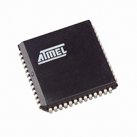
IC 8051 MCU FLASH 32K USB 52PLCC
Manufacturer
Atmel
Series
AT89C513xr
Datasheet
1.AT89C5130A-PUTUM.pdf
(188 pages)
Specifications of AT89C5131A-S3SUM
Core Processor
C52X2
Core Size
8-Bit
Speed
48MHz
Connectivity
I²C, SPI, UART/USART, USB
Peripherals
LED, POR, PWM, WDT
Number Of I /o
34
Program Memory Size
32KB (32K x 8)
Program Memory Type
FLASH
Eeprom Size
4K x 8
Ram Size
1.25K x 8
Voltage - Supply (vcc/vdd)
2.7 V ~ 5.5 V
Oscillator Type
Internal
Operating Temperature
-40°C ~ 85°C
Package / Case
52-PLCC
Processor Series
AT89x
Core
8051
Data Bus Width
8 bit
Data Ram Size
1.25 KB
Interface Type
2-Wire, EUART, SPI, USB
Maximum Clock Frequency
48 MHz
Number Of Programmable I/os
34
Number Of Timers
16 bit
Operating Supply Voltage
2.7 V to 5.5 V
Maximum Operating Temperature
+ 85 C
Mounting Style
SMD/SMT
3rd Party Development Tools
PK51, CA51, A51, ULINK2
Development Tools By Supplier
AT89STK-05
Minimum Operating Temperature
- 40 C
Package
52PLCC
Device Core
8051
Family Name
89C
Maximum Speed
48 MHz
For Use With
AT89OCD-01 - USB EMULATOR FOR AT8XC51 MCUAT89STK-10 - KIT EVAL APPL MASS STORAGEAT89STK-05 - KIT STARTER FOR AT89C5131
Lead Free Status / RoHS Status
Lead free / RoHS Compliant
Data Converters
-
Lead Free Status / Rohs Status
Details
Available stocks
Company
Part Number
Manufacturer
Quantity
Price
Company:

Part Number:
AT89C5131A-S3SUM
Manufacturer:
ATMEL
Quantity:
46


27.5
27.6
27.6.0.1
27.6.0.2
4337K–USB–04/08
USB AC Parameters
SPI Interface AC Parameters
Definition of Symbols
Timings
Differential
Data Lines
V
CRS
Table 27-14. USB AC Parameters
Table 27-15. SPI Interface Timing Symbol Definitions
Test conditions: capacitive load on all pins= 50 pF.
Table 27-16. SPI Interface Master AC Timing
C
I
O
Symbol
t
FDRATE
V
t
t
t
t
DJ1
DJ2
JR1
JR2
t
t
CRS
R
F
10%
Parameter
Rise Time
Fall Time
Full-speed Data Rate
Crossover Voltage
Source Jitter Total to Next
Transaction
Source Jitter Total for Paired
Transactions
Receiver Jitter to Next
Transaction
Receiver Jitter for Paired
Transactions
Rise Time
Signals
t
R
Clock
Data In
Data Out
90%
90%
11.9700
-18.5
Min
-3.5
1.3
-4
-9
4
4
Fall Time
t
F
Typ
10%
AT89C5130A/31A-M
H
L
V
X
Z
12.0300
Max
18.5
2.0
3.5
20
20
4
9
Conditions
Mb/s
Unit
ns
ns
ns
ns
ns
ns
V
High
Low
Valid
No Longer Valid
Floating
V
V
Hmin
Lmax
Test Conditions
173
Related parts for AT89C5131A-S3SUM
Image
Part Number
Description
Manufacturer
Datasheet
Request
R

Part Number:
Description:
Manufacturer:
Atmel Corporation
Datasheet:
Part Number:
Description:
Manufacturer:
Atmel Corporation
Datasheet:

Part Number:
Description:
IC 8051 MCU FLASH 32K USB 32QFN
Manufacturer:
Atmel
Datasheet:

Part Number:
Description:
IC MCU 32KB 3-3.6V USB 48-VQFN
Manufacturer:
Atmel
Datasheet:

Part Number:
Description:
MCU 8051 32K FLASH USB 28-SOIC
Manufacturer:
Atmel
Datasheet:

Part Number:
Description:
IC 8051 MCU FLASH 32K USB 64VQFP
Manufacturer:
Atmel
Datasheet:
Part Number:
Description:
MCU 8051 32K FLASH USB 64-VQFP
Manufacturer:
Atmel
Datasheet:
Part Number:
Description:
MCU 8051 32K FLASH USB 28-SOIC
Manufacturer:
Atmel
Datasheet:

Part Number:
Description:
MCU 8051 32K FLASH USB 52-PLCC
Manufacturer:
Atmel
Datasheet:
Part Number:
Description:
IC 8051 MCU FLASH 32K USB 48QFN
Manufacturer:
Atmel
Datasheet:
Part Number:
Description:
IC 8051 MCU FLASH 32K USB 64VQFP
Manufacturer:
Atmel
Datasheet:
Part Number:
Description:
IC 8051 MCU FLASH 32K USB 32QFN
Manufacturer:
Atmel
Datasheet:
Part Number:
Description:
IC 8051 MCU FLASH 32K USB 52PLCC
Manufacturer:
Atmel
Datasheet:
Part Number:
Description:
IC 8051 MCU FLASH 32K USB 28SOIC
Manufacturer:
Atmel
Datasheet: