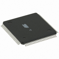
ATMEGA3250P-20AU Atmel, ATMEGA3250P-20AU Datasheet - Page 300

ATMEGA3250P-20AU
Manufacturer Part Number
ATMEGA3250P-20AU
Description
IC MCU AVR 32K FLASH 100-TQFP
Manufacturer
Atmel
Series
AVR® ATmegar
Specifications of ATMEGA3250P-20AU
Core Processor
AVR
Core Size
8-Bit
Speed
20MHz
Connectivity
SPI, UART/USART, USI
Peripherals
Brown-out Detect/Reset, POR, PWM, WDT
Number Of I /o
69
Program Memory Size
32KB (16K x 16)
Program Memory Type
FLASH
Eeprom Size
1K x 8
Ram Size
2K x 8
Voltage - Supply (vcc/vdd)
2.7 V ~ 5.5 V
Data Converters
A/D 8x10b
Oscillator Type
Internal
Operating Temperature
-40°C ~ 85°C
Package / Case
100-TQFP, 100-VQFP
Processor Series
ATMEGA32x
Core
AVR8
Data Bus Width
8 bit
Data Ram Size
2 KB
Interface Type
SPI/UART/USI
Maximum Clock Frequency
20 MHz
Number Of Programmable I/os
69
Number Of Timers
3
Maximum Operating Temperature
+ 85 C
Mounting Style
SMD/SMT
3rd Party Development Tools
EWAVR, EWAVR-BL
Development Tools By Supplier
ATAVRDRAGON, ATSTK500, ATSTK600, ATAVRISP2, ATAVRONEKIT
Minimum Operating Temperature
- 40 C
On-chip Adc
8-ch x 10-bit
For Use With
ATSTK600-TQFP100 - STK600 SOCKET/ADAPTER 100-TQFP770-1007 - ISP 4PORT ATMEL AVR MCU SPI/JTAG770-1005 - ISP 4PORT FOR ATMEL AVR MCU JTAG770-1004 - ISP 4PORT FOR ATMEL AVR MCU SPIATAVRISP2 - PROGRAMMER AVR IN SYSTEMATSTK504 - STARTER KIT AVR EXP MOD 100P LCD
Lead Free Status / RoHS Status
Lead free / RoHS Compliant
Other names
ATMEGA3250P-16AU
ATMEGA3250P-16AU
ATMEGA3250P-16AU
Available stocks
Company
Part Number
Manufacturer
Quantity
Price
Part Number:
ATMEGA3250P-20AU
Manufacturer:
AT
Quantity:
20 000
- Current page: 300 of 364
- Download datasheet (6Mb)
25.8.12
25.8.13
25.8.14
300
ATmega325P/3250P
Programming Algorithm
Entering Programming Mode
Leaving Programming Mode
ture-DR encountered after entering the PROG_PAGEREAD command. The Program Counter is
post-incremented after reading each high byte, including the first read byte. This ensures that
the first data is captured from the first address set up by PROG_COMMANDS, and reading the
last location in the page makes the program counter increment into the next page.
Figure 25-17. Flash Data Byte Register
The state machine controlling the Flash Data Byte Register is clocked by TCK. During normal
operation in which eight bits are shifted for each Flash byte, the clock cycles needed to navigate
through the TAP controller automatically feeds the state machine for the Flash Data Byte Regis-
ter with sufficient number of clock pulses to complete its operation transparently for the user.
However, if too few bits are shifted between each Update-DR state during page load, the TAP
controller should stay in the Run-Test/Idle state for some TCK cycles to ensure that there are at
least 11 TCK cycles between each Update-DR state.
All references below of type “1a”, “1b”, and so on, refer to
1. Enter JTAG instruction AVR_RESET and shift 1 in the Reset Register.
2. Enter instruction PROG_ENABLE and shift 0b1010_0011_0111_0000 in the Program-
1. Enter JTAG instruction PROG_COMMANDS.
2. Disable all programming instructions by using no operation instruction 11a.
3. Enter instruction PROG_ENABLE and shift 0b0000_0000_0000_0000 in the program-
4. Enter JTAG instruction AVR_RESET and shift 0 in the Reset Register.
ming Enable Register.
ming Enable Register.
TDO
TDI
D
A
T
A
Machine
State
STROBES
ADDRESS
Table
EEPROM
Lock Bits
Fuses
Flash
25-17.
8023F–AVR–07/09
Related parts for ATMEGA3250P-20AU
Image
Part Number
Description
Manufacturer
Datasheet
Request
R

Part Number:
Description:
Manufacturer:
Atmel Corporation
Datasheet:

Part Number:
Description:
IC AVR MCU 32K 16MHZ 100TQFP
Manufacturer:
Atmel
Datasheet:

Part Number:
Description:
IC AVR MCU 32K 16MHZ 100TQFP
Manufacturer:
Atmel
Datasheet:

Part Number:
Description:
MCU AVR 32K FLASH 16MHZ 100TQFP
Manufacturer:
Atmel
Datasheet:

Part Number:
Description:
Atmega3250 8-bit Microcontroller With In-system Programmable Flash
Manufacturer:
ATMEL Corporation

Part Number:
Description:
Manufacturer:
Atmel Corporation
Datasheet:

Part Number:
Description:
IC AVR MCU 32K 16MHZ 64-QFN
Manufacturer:
Atmel
Datasheet:

Part Number:
Description:
IC AVR MCU 32K 16MHZ 64TQFP
Manufacturer:
Atmel
Datasheet:

Part Number:
Description:
IC AVR MCU 32K 16MHZ 64TQFP
Manufacturer:
Atmel
Datasheet:

Part Number:
Description:
IC AVR MCU 32K 16MHZ 64-QFN
Manufacturer:
Atmel
Datasheet:

Part Number:
Description:
8-bit Microcontroller with In-System Programmable Flash
Manufacturer:
ATMEL [ATMEL Corporation]
Datasheet:

Part Number:
Description:
MCU AVR 32K FLASH 16MHZ 64TQFP
Manufacturer:
Atmel
Datasheet:

Part Number:
Description:
MCU AVR 32K FLASH 16MHZ 64QFN
Manufacturer:
Atmel
Datasheet:


