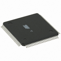
ATMEGA3250P-20AU Atmel, ATMEGA3250P-20AU Datasheet - Page 182

ATMEGA3250P-20AU
Manufacturer Part Number
ATMEGA3250P-20AU
Description
IC MCU AVR 32K FLASH 100-TQFP
Manufacturer
Atmel
Series
AVR® ATmegar
Specifications of ATMEGA3250P-20AU
Core Processor
AVR
Core Size
8-Bit
Speed
20MHz
Connectivity
SPI, UART/USART, USI
Peripherals
Brown-out Detect/Reset, POR, PWM, WDT
Number Of I /o
69
Program Memory Size
32KB (16K x 16)
Program Memory Type
FLASH
Eeprom Size
1K x 8
Ram Size
2K x 8
Voltage - Supply (vcc/vdd)
2.7 V ~ 5.5 V
Data Converters
A/D 8x10b
Oscillator Type
Internal
Operating Temperature
-40°C ~ 85°C
Package / Case
100-TQFP, 100-VQFP
Processor Series
ATMEGA32x
Core
AVR8
Data Bus Width
8 bit
Data Ram Size
2 KB
Interface Type
SPI/UART/USI
Maximum Clock Frequency
20 MHz
Number Of Programmable I/os
69
Number Of Timers
3
Maximum Operating Temperature
+ 85 C
Mounting Style
SMD/SMT
3rd Party Development Tools
EWAVR, EWAVR-BL
Development Tools By Supplier
ATAVRDRAGON, ATSTK500, ATSTK600, ATAVRISP2, ATAVRONEKIT
Minimum Operating Temperature
- 40 C
On-chip Adc
8-ch x 10-bit
For Use With
ATSTK600-TQFP100 - STK600 SOCKET/ADAPTER 100-TQFP770-1007 - ISP 4PORT ATMEL AVR MCU SPI/JTAG770-1005 - ISP 4PORT FOR ATMEL AVR MCU JTAG770-1004 - ISP 4PORT FOR ATMEL AVR MCU SPIATAVRISP2 - PROGRAMMER AVR IN SYSTEMATSTK504 - STARTER KIT AVR EXP MOD 100P LCD
Lead Free Status / RoHS Status
Lead free / RoHS Compliant
Other names
ATMEGA3250P-16AU
ATMEGA3250P-16AU
ATMEGA3250P-16AU
Available stocks
Company
Part Number
Manufacturer
Quantity
Price
Part Number:
ATMEGA3250P-20AU
Manufacturer:
AT
Quantity:
20 000
- Current page: 182 of 364
- Download datasheet (6Mb)
18.10 Register Description
18.10.1
18.10.2
182
ATmega325P/3250P
UDRn – USART I/O Data Register n
UCSRnA – USART Control and Status Register n A
The USART Transmit Data Buffer Register and USART Receive Data Buffer Registers share the
same I/O address referred to as USART Data Register or UDRn. The Transmit Data Buffer Reg-
ister (TXB) will be the destination for data written to the UDRn Register location. Reading the
UDRn Register location will return the contents of the Receive Data Buffer Register (RXB).
For 5-, 6-, or 7-bit characters the upper unused bits will be ignored by the Transmitter and set to
zero by the Receiver.
The transmit buffer can only be written when the UDREn Flag in the UCSRnA Register is set.
Data written to UDRn when the UDREn Flag is not set, will be ignored by the USART Transmit-
ter. When data is written to the transmit buffer, and the Transmitter is enabled, the Transmitter
will load the data into the Transmit Shift Register when the Shift Register is empty. Then the
data will be serially transmitted on the TxD pin.
The receive buffer consists of a two level FIFO. The FIFO will change its state whenever the
receive buffer is accessed. Due to this behavior of the receive buffer, do not use Read-Modify-
Write instructions (SBI and CBI) on this location. Be careful when using bit test instructions
(SBIC and SBIS), since these also will change the state of the FIFO.
• Bit 7 – RXCn: USART Receive Complete
This flag bit is set when there are unread data in the receive buffer and cleared when the receive
buffer is empty (i.e., does not contain any unread data). If the Receiver is disabled, the receive
buffer will be flushed and consequently the RXCn bit will become zero. The RXCn Flag can be
used to generate a Receive Complete interrupt (see description of the RXCIEn bit).
• Bit 6 – TXCn: USART Transmit Complete
This flag bit is set when the entire frame in the Transmit Shift Register has been shifted out and
there are no new data currently present in the transmit buffer (UDRn). The TXCn Flag bit is auto-
matically cleared when a transmit complete interrupt is executed, or it can be cleared by writing
a one to its bit location. The TXCn Flag can generate a Transmit Complete interrupt (see
description of the TXCIEn bit).
Bit
Read/Write
Initial Value
Bit
Read/Write
Initial Value
RXCn
R/W
R
7
0
7
0
TXCn
R/W
R/W
6
0
6
0
UDREn
R/W
5
0
R
5
1
R/W
4
0
FEn
RXBn[7:0]
R
TXBn[7:0]
4
0
R/W
3
0
DORn
R
3
0
R/W
2
0
UPEn
R
2
0
R/W
1
0
U2Xn
R/W
1
0
R/W
0
0
MPCMn
R/W
0
0
8023F–AVR–07/09
UDRn (Write)
UDRn (Read)
UCSRnA
Related parts for ATMEGA3250P-20AU
Image
Part Number
Description
Manufacturer
Datasheet
Request
R

Part Number:
Description:
Manufacturer:
Atmel Corporation
Datasheet:

Part Number:
Description:
IC AVR MCU 32K 16MHZ 100TQFP
Manufacturer:
Atmel
Datasheet:

Part Number:
Description:
IC AVR MCU 32K 16MHZ 100TQFP
Manufacturer:
Atmel
Datasheet:

Part Number:
Description:
MCU AVR 32K FLASH 16MHZ 100TQFP
Manufacturer:
Atmel
Datasheet:

Part Number:
Description:
Atmega3250 8-bit Microcontroller With In-system Programmable Flash
Manufacturer:
ATMEL Corporation

Part Number:
Description:
Manufacturer:
Atmel Corporation
Datasheet:

Part Number:
Description:
IC AVR MCU 32K 16MHZ 64-QFN
Manufacturer:
Atmel
Datasheet:

Part Number:
Description:
IC AVR MCU 32K 16MHZ 64TQFP
Manufacturer:
Atmel
Datasheet:

Part Number:
Description:
IC AVR MCU 32K 16MHZ 64TQFP
Manufacturer:
Atmel
Datasheet:

Part Number:
Description:
IC AVR MCU 32K 16MHZ 64-QFN
Manufacturer:
Atmel
Datasheet:

Part Number:
Description:
8-bit Microcontroller with In-System Programmable Flash
Manufacturer:
ATMEL [ATMEL Corporation]
Datasheet:

Part Number:
Description:
MCU AVR 32K FLASH 16MHZ 64TQFP
Manufacturer:
Atmel
Datasheet:

Part Number:
Description:
MCU AVR 32K FLASH 16MHZ 64QFN
Manufacturer:
Atmel
Datasheet:


