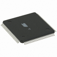
ATMEGA3250P-20AU Atmel, ATMEGA3250P-20AU Datasheet - Page 290

ATMEGA3250P-20AU
Manufacturer Part Number
ATMEGA3250P-20AU
Description
IC MCU AVR 32K FLASH 100-TQFP
Manufacturer
Atmel
Series
AVR® ATmegar
Specifications of ATMEGA3250P-20AU
Core Processor
AVR
Core Size
8-Bit
Speed
20MHz
Connectivity
SPI, UART/USART, USI
Peripherals
Brown-out Detect/Reset, POR, PWM, WDT
Number Of I /o
69
Program Memory Size
32KB (16K x 16)
Program Memory Type
FLASH
Eeprom Size
1K x 8
Ram Size
2K x 8
Voltage - Supply (vcc/vdd)
2.7 V ~ 5.5 V
Data Converters
A/D 8x10b
Oscillator Type
Internal
Operating Temperature
-40°C ~ 85°C
Package / Case
100-TQFP, 100-VQFP
Processor Series
ATMEGA32x
Core
AVR8
Data Bus Width
8 bit
Data Ram Size
2 KB
Interface Type
SPI/UART/USI
Maximum Clock Frequency
20 MHz
Number Of Programmable I/os
69
Number Of Timers
3
Maximum Operating Temperature
+ 85 C
Mounting Style
SMD/SMT
3rd Party Development Tools
EWAVR, EWAVR-BL
Development Tools By Supplier
ATAVRDRAGON, ATSTK500, ATSTK600, ATAVRISP2, ATAVRONEKIT
Minimum Operating Temperature
- 40 C
On-chip Adc
8-ch x 10-bit
For Use With
ATSTK600-TQFP100 - STK600 SOCKET/ADAPTER 100-TQFP770-1007 - ISP 4PORT ATMEL AVR MCU SPI/JTAG770-1005 - ISP 4PORT FOR ATMEL AVR MCU JTAG770-1004 - ISP 4PORT FOR ATMEL AVR MCU SPIATAVRISP2 - PROGRAMMER AVR IN SYSTEMATSTK504 - STARTER KIT AVR EXP MOD 100P LCD
Lead Free Status / RoHS Status
Lead free / RoHS Compliant
Other names
ATMEGA3250P-16AU
ATMEGA3250P-16AU
ATMEGA3250P-16AU
Available stocks
Company
Part Number
Manufacturer
Quantity
Price
Part Number:
ATMEGA3250P-20AU
Manufacturer:
AT
Quantity:
20 000
- Current page: 290 of 364
- Download datasheet (6Mb)
Figure 25-12. Serial Programming Instruction example
25.7.2
290
Byte 1
ATmega325P/3250P
SPI Serial Programming Characteristics
Load Program Memory Page (High/Low Byte)/
Load EEPROM Memory Page (page access)
Bit 15 B
Byte 2
Adr M M S S B
A
Notes:
If the LSB in RDY/BSY data byte out is ‘1’, a programming operation is still pending. Wait until
this bit returns ‘0’ before the next instruction is carried out.
Within the same page, the low data byte must be loaded prior to the high data byte.
After data is loaded to the page buffer, program the EEPROM page, see
For characteristics of the SPI module, see
Byte 3
Adr LSB
1. Not all instructions are applicable for all parts
2. a = address
3. Bits are programmed ‘0’, unprogrammed ‘1’.
4. To ensure future compatibility, unused Fuses and Lock bits should be unprogrammed (‘1’) .
5. Refer to the correspondig section for Fuse and Lock bits, Calibration and Signature bytes and
6. Instructions accessing program memory use word address. This address may be random
7. See htt://www.atmel.com/avr for Application Notes regarding programming and programmers.
Page size.
within the page range.
Page Offset
0
Serial Programming Instruction
Byte 4
Program Memory/
EEPROM Memory
Page Buffer
Page N-1
Page 0
Page 1
Page 2
Byte 1
”SPI Timing Characteristics” on page
Page Number
Bit 15 B
Byte 2
Write Program Memory Page/
Write EEPROM Memory Page
Adr MSB
Byte 3
A A dr r L L SB B
Figure
0
25-12.
310.
8023F–AVR–07/09
Byte 4
Related parts for ATMEGA3250P-20AU
Image
Part Number
Description
Manufacturer
Datasheet
Request
R

Part Number:
Description:
Manufacturer:
Atmel Corporation
Datasheet:

Part Number:
Description:
IC AVR MCU 32K 16MHZ 100TQFP
Manufacturer:
Atmel
Datasheet:

Part Number:
Description:
IC AVR MCU 32K 16MHZ 100TQFP
Manufacturer:
Atmel
Datasheet:

Part Number:
Description:
MCU AVR 32K FLASH 16MHZ 100TQFP
Manufacturer:
Atmel
Datasheet:

Part Number:
Description:
Atmega3250 8-bit Microcontroller With In-system Programmable Flash
Manufacturer:
ATMEL Corporation

Part Number:
Description:
Manufacturer:
Atmel Corporation
Datasheet:

Part Number:
Description:
IC AVR MCU 32K 16MHZ 64-QFN
Manufacturer:
Atmel
Datasheet:

Part Number:
Description:
IC AVR MCU 32K 16MHZ 64TQFP
Manufacturer:
Atmel
Datasheet:

Part Number:
Description:
IC AVR MCU 32K 16MHZ 64TQFP
Manufacturer:
Atmel
Datasheet:

Part Number:
Description:
IC AVR MCU 32K 16MHZ 64-QFN
Manufacturer:
Atmel
Datasheet:

Part Number:
Description:
8-bit Microcontroller with In-System Programmable Flash
Manufacturer:
ATMEL [ATMEL Corporation]
Datasheet:

Part Number:
Description:
MCU AVR 32K FLASH 16MHZ 64TQFP
Manufacturer:
Atmel
Datasheet:

Part Number:
Description:
MCU AVR 32K FLASH 16MHZ 64QFN
Manufacturer:
Atmel
Datasheet:


