AT91SAM7S32B-MU Atmel, AT91SAM7S32B-MU Datasheet - Page 615
AT91SAM7S32B-MU
Manufacturer Part Number
AT91SAM7S32B-MU
Description
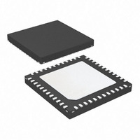
IC MCU ARM7 32KB FLASH 48-VQFN
Manufacturer
Atmel
Series
AT91SAMr
Datasheet
1.AT91SAM7S16-MU.pdf
(779 pages)
Specifications of AT91SAM7S32B-MU
Core Processor
ARM7
Core Size
16/32-Bit
Speed
55MHz
Connectivity
I²C, SPI, SSC, UART/USART
Peripherals
Brown-out Detect/Reset, DMA, POR, PWM, WDT
Number Of I /o
21
Program Memory Size
32KB (32K x 8)
Program Memory Type
FLASH
Ram Size
8K x 8
Voltage - Supply (vcc/vdd)
1.65 V ~ 1.95 V
Data Converters
A/D 8x10b
Oscillator Type
Internal
Operating Temperature
-40°C ~ 85°C
Package / Case
48-VQFN Exposed Pad, 48-HVQFN, 48-SQFN, 48-DHVQFN
For Use With
AT91SAM-ICE - EMULATOR FOR AT91 ARM7/ARM9AT91SAM7S-EK - KIT EVAL FOR ARM AT91SAM7S
Lead Free Status / RoHS Status
Lead free / RoHS Compliant
Eeprom Size
-
Available stocks
Company
Part Number
Manufacturer
Quantity
Price


40.6.2.11
40.6.3
40.6.3.1
40.6.4
40.6.4.1
6175K–ATARM–30-Aug-10
Master Clock (MCK)
Non Volatile Memory Bits (NVM Bits)
ADC: Sleep Mode
MCK: Limited Master Clock Frequency Ranges
NVM Bits: Write/Erase Cycles Number
None.
If Sleep mode is activated while there is no activity (no conversion is being performed), it will
take effect only after a conversion occurs.
To activate sleep mode as soon as possible, it is recommended to write successively, ADC
Mode Register (SLEEP) then ADC Control Register (START bit field); to start an analog-to-digi-
tal conversion, in order put ADC into sleep mode at the end of this conversion.
If the Flash is operating without wait states, the frequency of the Master Clock MCK must be
lower than 3 MHz or higher than 19 MHz.
If the Flash is operating with one wait state, the frequency of the Master Clock MCK must be
lower than 3 MHz or higher than 19 MHz.
If the Flash is operating with two wait states, the frequency of the Master Clock MCK must be
lower than 3 MHz or higher than 25 MHz.
If the Flash is operating with three wait states, the frequency of the Master Clock MCK must be
lower than 3 MHz or higher than 38 MHz.
If these constraints are not respected, the correct operation of the system cannot be guaranteed
and either data or prefetch abort might occur.
The maximum operating frequencies (at 30 MHz @ 0 Wait States and 55 MHz @ 1 Wait State)
as stated in
Note:
The user must ensure that the device is running at the authorized frequency by programming the
PLL properly to not run within the forbidden frequency range.
The maximum number of write/erase cycles for Non Volatile Memory bits is 100. This includes
Lock Bits (LOCKx), General Purpose NVM bits (GPNVMx) and the Security Bit.
This maximum number of write/erase cycles is not applicable to 256 KB Flash memory, it
remains at 10K for the Flash memory.
None.
Problem Fix/Workaround
Problem Fix/Workaround
Problem Fix/Workaround
Problem Fix/Workaround
It is not necessary to use 2 o 3 wait states because the Flash can operate at maximum frequency
with only 1 wait state.
Table 37-24, “Embedded Flash Wait States,” on page
AT91SAM7S Series Preliminary
578, are still applicable.
615
Related parts for AT91SAM7S32B-MU
Image
Part Number
Description
Manufacturer
Datasheet
Request
R

Part Number:
Description:
KIT EVAL FOR ARM AT91SAM7S
Manufacturer:
Atmel
Datasheet:

Part Number:
Description:
MCU, MPU & DSP Development Tools KICKSTART KIT ATMEL AT91SAM7S
Manufacturer:
IAR Systems

Part Number:
Description:
DEV KIT FOR AVR/AVR32
Manufacturer:
Atmel
Datasheet:

Part Number:
Description:
INTERVAL AND WIPE/WASH WIPER CONTROL IC WITH DELAY
Manufacturer:
ATMEL Corporation
Datasheet:
Part Number:
Description:
Low-Voltage Voice-Switched IC for Hands-Free Operation
Manufacturer:
ATMEL Corporation
Datasheet:
Part Number:
Description:
MONOLITHIC INTEGRATED FEATUREPHONE CIRCUIT
Manufacturer:
ATMEL Corporation
Datasheet:
Part Number:
Description:
AM-FM Receiver IC U4255BM-M
Manufacturer:
ATMEL Corporation
Datasheet:
Part Number:
Description:
Monolithic Integrated Feature Phone Circuit
Manufacturer:
ATMEL Corporation
Datasheet:
Part Number:
Description:
Multistandard Video-IF and Quasi Parallel Sound Processing
Manufacturer:
ATMEL Corporation
Datasheet:
Part Number:
Description:
High-performance EE PLD
Manufacturer:
ATMEL Corporation
Datasheet:
Part Number:
Description:
8-bit Flash Microcontroller
Manufacturer:
ATMEL Corporation
Datasheet:
Part Number:
Description:
2-Wire Serial EEPROM
Manufacturer:
ATMEL Corporation
Datasheet: