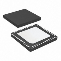
AT91SAM7S32B-MU Atmel, AT91SAM7S32B-MU Datasheet - Page 577

AT91SAM7S32B-MU
Manufacturer Part Number
AT91SAM7S32B-MU
Description
IC MCU ARM7 32KB FLASH 48-VQFN
Manufacturer
Atmel
Series
AT91SAMr
Datasheet
1.AT91SAM7S16-MU.pdf
(779 pages)
Specifications of AT91SAM7S32B-MU
Core Processor
ARM7
Core Size
16/32-Bit
Speed
55MHz
Connectivity
I²C, SPI, SSC, UART/USART
Peripherals
Brown-out Detect/Reset, DMA, POR, PWM, WDT
Number Of I /o
21
Program Memory Size
32KB (32K x 8)
Program Memory Type
FLASH
Ram Size
8K x 8
Voltage - Supply (vcc/vdd)
1.65 V ~ 1.95 V
Data Converters
A/D 8x10b
Oscillator Type
Internal
Operating Temperature
-40°C ~ 85°C
Package / Case
48-VQFN Exposed Pad, 48-HVQFN, 48-SQFN, 48-DHVQFN
For Use With
AT91SAM-ICE - EMULATOR FOR AT91 ARM7/ARM9AT91SAM7S-EK - KIT EVAL FOR ARM AT91SAM7S
Lead Free Status / RoHS Status
Lead free / RoHS Compliant
Eeprom Size
-
Available stocks
Company
Part Number
Manufacturer
Quantity
Price
- Current page: 577 of 779
- Download datasheet (11Mb)
Table 37-23. SSC Timings (Continued)
Notes:
6175K–ATARM–30-Aug-10
Symbol
SSC
SSC
SSC
SSC
SSC
SSC
SSC
SSC
6
7
8
9
10
11
12
13
(1)
1. Timings SSC4 and SSC7 depend on the start condition. When STTDLY = 0 (Receive start delay) and START = 4, or 5 or 7
2. For output signals (TF, TD, RF), Min and Max access times are defined. The Min access time is the time between the TK (or
3. 3.3V domain: V
4. 1.8V domain: V
5. t
(Receive Start Selection), two Periods of the MCK must be added to timings.
RK) edge and the signal change. The Max access timing is the time between the TK edge and the signal stabilization.
37-16
Parameter
TF hold time after TK edge (TK input)
TK edge to TF/TD (TK input, TF input)
RF/RD setup time before RK edge (RK input)
RF/RD hold time after RK edge (RK input)
RK edge to RF (RK input)
RF/RD setup time before RK edge (RK output)
RF/RD hold time after RK edge (RK output)
RK edge to RF (RK output)
CPMCK
illustrates Min and Max accesses for SSC0. The same applies for SSC1, SSC4, and SSC7, SSC10 and SSC13.
: Master Clock period in ns
VDDIO
VDDIO
Figure 37-16. Min and Max access time of output signals
from 3.0V to 3.6V, maximum external capacitor = 40 pF.
from 1.65V to 1.95V, maximum external capacitor = 20 pF.
TK (CKI =0)
TK (CKI =1)
TF/TD
Receiver
Conditions
3.3V domain
1.8V domain
3.3V domain
1.8V domain
3.3V domain
1.8V domain
3.3V domain
1.8V domain
3.3V domain
1.8V domain
3.3V domain
1.8V domain
3.3V domain
1.8V domain
3.3V domain
1.8V domain
AT91SAM7S Series Preliminary
SSC
SSC
0max
0min
10 (+3*t
6 (+3*t
56.5 - t
t
26 - t
t
CPMCK
CPMCK
t
t
t
t
10.5
CPMCK
CPMCK
CPMCK
CPMCK
Min
CPMCK
6
0
0
CPMCK
0
0
(2)
CPMCK
(2)
(2)
CPMCK
(2)
- 5.5
- 10
)
(1)(2)
)
(1)(2)
29.5 (+3*t
56 (+3*t
Max
27
58
12
4
CPMCK
(2)
CPMCK
(2)
(2)
(2)
)
(1)(2)
)
(1)(2)
Units
Figure
ns
ns
ns
ns
ns
ns
ns
ns
ns
ns
ns
ns
ns
ns
ns
ns
577
Related parts for AT91SAM7S32B-MU
Image
Part Number
Description
Manufacturer
Datasheet
Request
R

Part Number:
Description:
KIT EVAL FOR ARM AT91SAM7S
Manufacturer:
Atmel
Datasheet:

Part Number:
Description:
MCU, MPU & DSP Development Tools KICKSTART KIT ATMEL AT91SAM7S
Manufacturer:
IAR Systems

Part Number:
Description:
DEV KIT FOR AVR/AVR32
Manufacturer:
Atmel
Datasheet:

Part Number:
Description:
INTERVAL AND WIPE/WASH WIPER CONTROL IC WITH DELAY
Manufacturer:
ATMEL Corporation
Datasheet:

Part Number:
Description:
Low-Voltage Voice-Switched IC for Hands-Free Operation
Manufacturer:
ATMEL Corporation
Datasheet:

Part Number:
Description:
MONOLITHIC INTEGRATED FEATUREPHONE CIRCUIT
Manufacturer:
ATMEL Corporation
Datasheet:

Part Number:
Description:
AM-FM Receiver IC U4255BM-M
Manufacturer:
ATMEL Corporation
Datasheet:

Part Number:
Description:
Monolithic Integrated Feature Phone Circuit
Manufacturer:
ATMEL Corporation
Datasheet:

Part Number:
Description:
Multistandard Video-IF and Quasi Parallel Sound Processing
Manufacturer:
ATMEL Corporation
Datasheet:

Part Number:
Description:
High-performance EE PLD
Manufacturer:
ATMEL Corporation
Datasheet:

Part Number:
Description:
8-bit Flash Microcontroller
Manufacturer:
ATMEL Corporation
Datasheet:

Part Number:
Description:
2-Wire Serial EEPROM
Manufacturer:
ATMEL Corporation
Datasheet:


