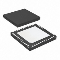
AT91SAM7S32B-MU Atmel, AT91SAM7S32B-MU Datasheet - Page 217

AT91SAM7S32B-MU
Manufacturer Part Number
AT91SAM7S32B-MU
Description
IC MCU ARM7 32KB FLASH 48-VQFN
Manufacturer
Atmel
Series
AT91SAMr
Datasheet
1.AT91SAM7S16-MU.pdf
(779 pages)
Specifications of AT91SAM7S32B-MU
Core Processor
ARM7
Core Size
16/32-Bit
Speed
55MHz
Connectivity
I²C, SPI, SSC, UART/USART
Peripherals
Brown-out Detect/Reset, DMA, POR, PWM, WDT
Number Of I /o
21
Program Memory Size
32KB (32K x 8)
Program Memory Type
FLASH
Ram Size
8K x 8
Voltage - Supply (vcc/vdd)
1.65 V ~ 1.95 V
Data Converters
A/D 8x10b
Oscillator Type
Internal
Operating Temperature
-40°C ~ 85°C
Package / Case
48-VQFN Exposed Pad, 48-HVQFN, 48-SQFN, 48-DHVQFN
For Use With
AT91SAM-ICE - EMULATOR FOR AT91 ARM7/ARM9AT91SAM7S-EK - KIT EVAL FOR ARM AT91SAM7S
Lead Free Status / RoHS Status
Lead free / RoHS Compliant
Eeprom Size
-
Available stocks
Company
Part Number
Manufacturer
Quantity
Price
- Current page: 217 of 779
- Download datasheet (11Mb)
26.3
26.3.1
26.3.2
26.3.3
26.4
26.4.1
6175K–ATARM–30-Aug-10
Product Dependencies
UART Operations
I/O Lines
Power Management
Interrupt Source
Baud Rate Generator
Depending on product integration, the Debug Unit pins may be multiplexed with PIO lines. In this
case, the programmer must first configure the corresponding PIO Controller to enable I/O lines
operations of the Debug Unit.
Depending on product integration, the Debug Unit clock may be controllable through the Power
Management Controller. In this case, the programmer must first configure the PMC to enable the
Debug Unit clock. Usually, the peripheral identifier used for this purpose is 1.
Depending on product integration, the Debug Unit interrupt line is connected to one of the inter-
rupt sources of the Advanced Interrupt Controller. Interrupt handling requires programming of
the AIC before configuring the Debug Unit. Usually, the Debug Unit interrupt line connects to the
interrupt source 1 of the AIC, which may be shared with the real-time clock, the system timer
interrupt lines and other system peripheral interrupts, as shown in
requires the programmer to determine the source of the interrupt when the source 1 is triggered.
The Debug Unit operates as a UART, (asynchronous mode only) and supports only 8-bit charac-
ter handling (with parity). It has no clock pin.
The Debug Unit's UART is made up of a receiver and a transmitter that operate independently,
and a common baud rate generator. Receiver timeout and transmitter time guard are not imple-
mented. However, all the implemented features are compatible with those of a standard USART.
The baud rate generator provides the bit period clock named baud rate clock to both the receiver
and the transmitter.
The baud rate clock is the master clock divided by 16 times the value (CD) written in
DBGU_BRGR (Baud Rate Generator Register). If DBGU_BRGR is set to 0, the baud rate clock
is disabled and the Debug Unit's UART remains inactive. The maximum allowable baud rate is
Master Clock divided by 16. The minimum allowable baud rate is Master Clock divided by (16 x
65536).
AT91SAM7S Series Preliminary
Baud Rate
=
--------------------- -
16
MCK
×
CD
Figure
26-1. This sharing
217
Related parts for AT91SAM7S32B-MU
Image
Part Number
Description
Manufacturer
Datasheet
Request
R

Part Number:
Description:
KIT EVAL FOR ARM AT91SAM7S
Manufacturer:
Atmel
Datasheet:

Part Number:
Description:
MCU, MPU & DSP Development Tools KICKSTART KIT ATMEL AT91SAM7S
Manufacturer:
IAR Systems

Part Number:
Description:
DEV KIT FOR AVR/AVR32
Manufacturer:
Atmel
Datasheet:

Part Number:
Description:
INTERVAL AND WIPE/WASH WIPER CONTROL IC WITH DELAY
Manufacturer:
ATMEL Corporation
Datasheet:

Part Number:
Description:
Low-Voltage Voice-Switched IC for Hands-Free Operation
Manufacturer:
ATMEL Corporation
Datasheet:

Part Number:
Description:
MONOLITHIC INTEGRATED FEATUREPHONE CIRCUIT
Manufacturer:
ATMEL Corporation
Datasheet:

Part Number:
Description:
AM-FM Receiver IC U4255BM-M
Manufacturer:
ATMEL Corporation
Datasheet:

Part Number:
Description:
Monolithic Integrated Feature Phone Circuit
Manufacturer:
ATMEL Corporation
Datasheet:

Part Number:
Description:
Multistandard Video-IF and Quasi Parallel Sound Processing
Manufacturer:
ATMEL Corporation
Datasheet:

Part Number:
Description:
High-performance EE PLD
Manufacturer:
ATMEL Corporation
Datasheet:

Part Number:
Description:
8-bit Flash Microcontroller
Manufacturer:
ATMEL Corporation
Datasheet:

Part Number:
Description:
2-Wire Serial EEPROM
Manufacturer:
ATMEL Corporation
Datasheet:


