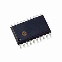
DSPIC33FJ12MC201-I/SO Microchip Technology, DSPIC33FJ12MC201-I/SO Datasheet - Page 57

DSPIC33FJ12MC201-I/SO
Manufacturer Part Number
DSPIC33FJ12MC201-I/SO
Description
IC DSPIC MCU/DSP 12K 20SOIC
Manufacturer
Microchip Technology
Series
dsPIC™ 33Fr
Datasheets
1.PIC24HJ12GP201-ISO.pdf
(84 pages)
2.DSPIC33FJ12MC201-ISO.pdf
(288 pages)
3.DSPIC33FJ12MC201-ISO.pdf
(14 pages)
4.DSPIC33FJ12MC201-IP.pdf
(284 pages)
Specifications of DSPIC33FJ12MC201-I/SO
Program Memory Type
FLASH
Program Memory Size
12KB (12K x 8)
Package / Case
20-SOIC (7.5mm Width)
Core Processor
dsPIC
Core Size
16-Bit
Speed
40 MIPs
Connectivity
I²C, IrDA, SPI, UART/USART
Peripherals
Brown-out Detect/Reset, Motor Control PWM, QEI, POR, PWM, WDT
Number Of I /o
15
Ram Size
1K x 8
Voltage - Supply (vcc/vdd)
3 V ~ 3.6 V
Data Converters
A/D 4x10b
Oscillator Type
Internal
Operating Temperature
-40°C ~ 85°C
Product
DSCs
Data Bus Width
16 bit
Processor Series
DSPIC33F
Core
dsPIC
Maximum Clock Frequency
40 MHz
Number Of Programmable I/os
15
Data Ram Size
1 KB
Maximum Operating Temperature
+ 85 C
Mounting Style
SMD/SMT
3rd Party Development Tools
52713-733, 52714-737, 53276-922, EWDSPIC
Development Tools By Supplier
PG164130, DV164035, DV244005, DV164005, PG164120, DM240001, DV164033
Minimum Operating Temperature
- 40 C
Lead Free Status / RoHS Status
Lead free / RoHS Compliant
For Use With
DV164033 - KIT START EXPLORER 16 MPLAB ICD2DM240001 - BOARD DEMO PIC24/DSPIC33/PIC32
Eeprom Size
-
Lead Free Status / Rohs Status
Lead free / RoHS Compliant
- PIC24HJ12GP201-ISO PDF datasheet
- DSPIC33FJ12MC201-ISO PDF datasheet #2
- DSPIC33FJ12MC201-ISO PDF datasheet #3
- DSPIC33FJ12MC201-IP PDF datasheet #4
- Current page: 57 of 284
- Download datasheet (5Mb)
5.0
The Reset module combines all Reset sources and
controls the device Master Reset Signal, SYSRST. The
following is a list of device Reset sources:
• POR: Power-on Reset
• BOR: Brown-out Reset
• MCLR: Master Clear Pin Reset
• SWR: RESET Instruction
• WDTO: Watchdog Timer Reset
• TRAPR: Trap Conflict Reset
• IOPUWR: Illegal Opcode, Uninitialized W
• CM: Configuration Mismatch Reset
A simplified block diagram of the Reset module is
shown in Figure 5-1.
FIGURE 5-1:
© 2007 Microchip Technology Inc.
Note:
Register Reset and Security Reset
RESETS
This data sheet summarizes the features
of the dsPIC33FJ12MC201/202 devices.
It is not intended to be a comprehensive
reference source. To complement the
information in this data sheet, refer to the
“dsPIC33F Family Reference Manual”.
Please see the Microchip web site
(www.microchip.com)
dsPIC33F
chapters.
MCLR
V
DD
Uninitialized W Register
Configuration Mismatch
RESET SYSTEM BLOCK DIAGRAM
Family
Regulator
RESET Instruction
Internal
Sleep or Idle
Illegal Opcode
Module
WDT
Trap Conflict
Reference
for
V
Detect
DD
the
Glitch Filter
Rise
Manual
latest
Preliminary
BOR
POR
dsPIC33FJ12MC201/202
Any active source of Reset makes the SYSRST signal
active. Many registers associated with the CPU and
peripherals are forced to a known Reset state. Most
registers are unaffected by a Reset; their status is
unknown on POR and unchanged by all other Resets.
All types of device Reset will set a corresponding status
bit in the RCON register to indicate the type of Reset
(see Register 5-1). A POR will clear all bits, except for
the POR bit (RCON<0>), that are set. The user
application can set or clear any bit at any time during
code execution. The RCON bits only serve as status
bits. Setting a particular Reset status bit in software
does not cause a device Reset to occur.
The RCON register also has other bits associated with
the Watchdog Timer and device power-saving states.
The function of these bits is discussed in other sections
of this manual.
Note:
Note:
Refer to the specific peripheral or CPU
section of this manual for register Reset
states.
The status bits in the RCON register
should be cleared after they are read so
that the next RCON register value after a
device Reset will be meaningful.
SYSRST
DS70265B-page 55
Related parts for DSPIC33FJ12MC201-I/SO
Image
Part Number
Description
Manufacturer
Datasheet
Request
R

Part Number:
Description:
IC, DSC, 16BIT, 12KB, 40MHZ, 3.6V, DIP28
Manufacturer:
Microchip Technology
Datasheet:

Part Number:
Description:
Manufacturer:
Microchip Technology Inc.
Datasheet:

Part Number:
Description:
Manufacturer:
Microchip Technology Inc.
Datasheet:

Part Number:
Description:
Manufacturer:
Microchip Technology Inc.
Datasheet:

Part Number:
Description:
Manufacturer:
Microchip Technology Inc.
Datasheet:

Part Number:
Description:
Manufacturer:
Microchip Technology Inc.
Datasheet:

Part Number:
Description:
Manufacturer:
Microchip Technology Inc.
Datasheet:

Part Number:
Description:
Manufacturer:
Microchip Technology Inc.
Datasheet:

Part Number:
Description:
Manufacturer:
Microchip Technology Inc.
Datasheet:


