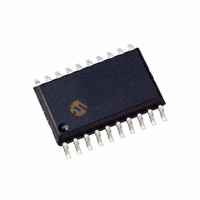
DSPIC33FJ12MC201-I/SO Microchip Technology, DSPIC33FJ12MC201-I/SO Datasheet - Page 107

DSPIC33FJ12MC201-I/SO
Manufacturer Part Number
DSPIC33FJ12MC201-I/SO
Description
IC DSPIC MCU/DSP 12K 20SOIC
Manufacturer
Microchip Technology
Series
dsPIC™ 33Fr
Datasheets
1.PIC24HJ12GP201-ISO.pdf
(84 pages)
2.DSPIC33FJ12MC201-ISO.pdf
(288 pages)
3.DSPIC33FJ12MC201-ISO.pdf
(14 pages)
4.DSPIC33FJ12MC201-IP.pdf
(284 pages)
Specifications of DSPIC33FJ12MC201-I/SO
Program Memory Type
FLASH
Program Memory Size
12KB (12K x 8)
Package / Case
20-SOIC (7.5mm Width)
Core Processor
dsPIC
Core Size
16-Bit
Speed
40 MIPs
Connectivity
I²C, IrDA, SPI, UART/USART
Peripherals
Brown-out Detect/Reset, Motor Control PWM, QEI, POR, PWM, WDT
Number Of I /o
15
Ram Size
1K x 8
Voltage - Supply (vcc/vdd)
3 V ~ 3.6 V
Data Converters
A/D 4x10b
Oscillator Type
Internal
Operating Temperature
-40°C ~ 85°C
Product
DSCs
Data Bus Width
16 bit
Processor Series
DSPIC33F
Core
dsPIC
Maximum Clock Frequency
40 MHz
Number Of Programmable I/os
15
Data Ram Size
1 KB
Maximum Operating Temperature
+ 85 C
Mounting Style
SMD/SMT
3rd Party Development Tools
52713-733, 52714-737, 53276-922, EWDSPIC
Development Tools By Supplier
PG164130, DV164035, DV244005, DV164005, PG164120, DM240001, DV164033
Minimum Operating Temperature
- 40 C
Lead Free Status / RoHS Status
Lead free / RoHS Compliant
For Use With
DV164033 - KIT START EXPLORER 16 MPLAB ICD2DM240001 - BOARD DEMO PIC24/DSPIC33/PIC32
Eeprom Size
-
Lead Free Status / Rohs Status
Lead free / RoHS Compliant
- PIC24HJ12GP201-ISO PDF datasheet
- DSPIC33FJ12MC201-ISO PDF datasheet #2
- DSPIC33FJ12MC201-ISO PDF datasheet #3
- DSPIC33FJ12MC201-IP PDF datasheet #4
- Current page: 107 of 284
- Download datasheet (5Mb)
9.0
All of the device pins (except V
OSC1/CLKI) are shared among the peripherals and the
parallel I/O ports. All I/O input ports feature Schmitt
Trigger inputs for improved noise immunity.
9.1
Generally a parallel I/O port that shares a pin with a
peripheral is subservient to the peripheral. The
peripheral’s output buffer data and control signals are
provided to a pair of multiplexers. The multiplexers
select whether the peripheral or the associated port
has ownership of the output data and control signals of
the I/O pin. The logic also prevents “loop through,” in
which a port’s digital output can drive the input of a
peripheral that shares the same pin. Figure 9-1 shows
how ports are shared with other peripherals and the
associated I/O pin to which they are connected.
FIGURE 9-1:
© 2007 Microchip Technology Inc.
Note:
I/O PORTS
Parallel I/O (PIO) Ports
This data sheet summarizes the features
of the dsPIC33FJ12MC201/202 devices.
It is not intended to be a comprehensive
reference source. To complement the
information in this data sheet, refer to the
“dsPIC33F Family Reference Manual”.
Please see the Microchip web site
(www.microchip.com)
dsPIC33F
chapters.
Read Port
Read LAT
Read TRIS
Data Bus
WR TRIS
WR LAT +
WR Port
BLOCK DIAGRAM OF A TYPICAL SHARED PORT STRUCTURE
Family
Peripheral Output Enable
Peripheral Output Data
Peripheral Input Data
Peripheral Module Enable
Peripheral Module
PIO Module
DD
Reference
TRIS Latch
Data Latch
D
D
CK
CK
, V
for
SS
Q
Q
, MCLR and
the
Manual
latest
Preliminary
dsPIC33FJ12MC201/202
Output Multiplexers
When a peripheral is enabled and the peripheral is
actively driving an associated pin, the use of the pin as
a general purpose output pin is disabled. The I/O pin
can be read, but the output driver for the parallel port bit
is disabled. If a peripheral is enabled, but the peripheral
is not actively driving a pin, that pin can be driven by a
port.
All port pins have three registers directly associated
with their operation as digital I/O. The data direction
register (TRISx) determines whether the pin is an input
or an output. If the data direction bit is a ‘1’, then the pin
is an input. All port pins are defined as inputs after a
Reset. Reads from the latch (LATx) read the latch.
Writes to the latch write the latch. Reads from the port
(PORTx) read the port pins, while writes to the port pins
write the latch.
Any bit and its associated data and control registers
that are not valid for a particular device will be
disabled. That means the corresponding LATx and
TRISx registers and the port pin will read as zeros.
When a pin is shared with another peripheral or
function that is defined as an input only, it is
nevertheless regarded as a dedicated port because
there is no other competing source of outputs.
1
0
1
0
Output Enable
Output Data
Input Data
I/O
I/O Pin
DS70265B-page 105
Related parts for DSPIC33FJ12MC201-I/SO
Image
Part Number
Description
Manufacturer
Datasheet
Request
R

Part Number:
Description:
IC, DSC, 16BIT, 12KB, 40MHZ, 3.6V, DIP28
Manufacturer:
Microchip Technology
Datasheet:

Part Number:
Description:
Manufacturer:
Microchip Technology Inc.
Datasheet:

Part Number:
Description:
Manufacturer:
Microchip Technology Inc.
Datasheet:

Part Number:
Description:
Manufacturer:
Microchip Technology Inc.
Datasheet:

Part Number:
Description:
Manufacturer:
Microchip Technology Inc.
Datasheet:

Part Number:
Description:
Manufacturer:
Microchip Technology Inc.
Datasheet:

Part Number:
Description:
Manufacturer:
Microchip Technology Inc.
Datasheet:

Part Number:
Description:
Manufacturer:
Microchip Technology Inc.
Datasheet:

Part Number:
Description:
Manufacturer:
Microchip Technology Inc.
Datasheet:


