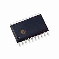
DSPIC33FJ12MC201-I/SO Microchip Technology, DSPIC33FJ12MC201-I/SO Datasheet - Page 210

DSPIC33FJ12MC201-I/SO
Manufacturer Part Number
DSPIC33FJ12MC201-I/SO
Description
IC DSPIC MCU/DSP 12K 20SOIC
Manufacturer
Microchip Technology
Series
dsPIC™ 33Fr
Datasheets
1.PIC24HJ12GP201-ISO.pdf
(84 pages)
2.DSPIC33FJ12MC201-ISO.pdf
(288 pages)
3.DSPIC33FJ12MC201-ISO.pdf
(14 pages)
4.DSPIC33FJ12MC201-IP.pdf
(284 pages)
Specifications of DSPIC33FJ12MC201-I/SO
Program Memory Type
FLASH
Program Memory Size
12KB (12K x 8)
Package / Case
20-SOIC (7.5mm Width)
Core Processor
dsPIC
Core Size
16-Bit
Speed
40 MIPs
Connectivity
I²C, IrDA, SPI, UART/USART
Peripherals
Brown-out Detect/Reset, Motor Control PWM, QEI, POR, PWM, WDT
Number Of I /o
15
Ram Size
1K x 8
Voltage - Supply (vcc/vdd)
3 V ~ 3.6 V
Data Converters
A/D 4x10b
Oscillator Type
Internal
Operating Temperature
-40°C ~ 85°C
Product
DSCs
Data Bus Width
16 bit
Processor Series
DSPIC33F
Core
dsPIC
Maximum Clock Frequency
40 MHz
Number Of Programmable I/os
15
Data Ram Size
1 KB
Maximum Operating Temperature
+ 85 C
Mounting Style
SMD/SMT
3rd Party Development Tools
52713-733, 52714-737, 53276-922, EWDSPIC
Development Tools By Supplier
PG164130, DV164035, DV244005, DV164005, PG164120, DM240001, DV164033
Minimum Operating Temperature
- 40 C
Lead Free Status / RoHS Status
Lead free / RoHS Compliant
For Use With
DV164033 - KIT START EXPLORER 16 MPLAB ICD2DM240001 - BOARD DEMO PIC24/DSPIC33/PIC32
Eeprom Size
-
Lead Free Status / Rohs Status
Lead free / RoHS Compliant
- PIC24HJ12GP201-ISO PDF datasheet
- DSPIC33FJ12MC201-ISO PDF datasheet #2
- DSPIC33FJ12MC201-ISO PDF datasheet #3
- DSPIC33FJ12MC201-IP PDF datasheet #4
- Current page: 210 of 284
- Download datasheet (5Mb)
dsPIC33FJ12MC201/202
REGISTER 19-5:
DS70265B-page 208
bit 15
bit 7
Legend:
R = Readable bit
-n = Value at POR
bit 15
bit 14-13
bit 12-8
bit 7
bit 6-5
bit 4-0
CH0NB
CH0NA
R/W-0
R/W-0
CH0NB: Channel 0 Negative Input Select for Sample B bit
1 = Channel 0 negative input is AN1
0 = Channel 0 negative input is V
Unimplemented: Read as ‘0’
CH0SB<4:0>: Channel 0 Positive Input Select for Sample B bits
01001 = Channel 0 positive input is AN9
01000 = Channel 0 positive input is AN8
•
•
•
00010 = Channel 0 positive input is AN2
00001 = Channel 0 positive input is AN1
00000 = Channel 0 positive input is AN0
CH0NA: Channel 0 Negative Input Select for Sample A bit
1 = Channel 0 negative input is AN1
0 = Channel 0 negative input is V
Unimplemented: Read as ‘0’
CH0SA<4:0>: Channel 0 Positive Input Select for Sample A bits
dsPIC33FJ12MC201 devices only:
00011 = Channel 0 positive input is AN3
00010 = Channel 0 positive input is AN2
00001 = Channel 0 positive input is AN1
00000 = Channel 0 positive input is AN0
dsPIC33FJ12MC202 devices only:
00101 = Channel 0 positive input is AN5
00100 = Channel 0 positive input is AN4
00011 = Channel 0 positive input is AN3
00010 = Channel 0 positive input is AN2
00001 = Channel 0 positive input is AN1
00000 = Channel 0 positive input is AN0
U-0
U-0
—
—
AD1CHS0: ADC1 INPUT CHANNEL 0 SELECT REGISTER
W = Writable bit
‘1’ = Bit is set
U-0
U-0
—
—
R/W-0
R/W-0
REF
REF
Preliminary
-
-
U = Unimplemented bit, read as ‘0’
‘0’ = Bit is cleared
R/W-0
R/W-0
CH0SB<4:0>
CH0SA<4:0>
R/W-0
R/W-0
© 2007 Microchip Technology Inc.
x = Bit is unknown
R/W-0
R/W-0
R/W-0
R/W-0
bit 8
bit 0
Related parts for DSPIC33FJ12MC201-I/SO
Image
Part Number
Description
Manufacturer
Datasheet
Request
R

Part Number:
Description:
IC, DSC, 16BIT, 12KB, 40MHZ, 3.6V, DIP28
Manufacturer:
Microchip Technology
Datasheet:

Part Number:
Description:
Manufacturer:
Microchip Technology Inc.
Datasheet:

Part Number:
Description:
Manufacturer:
Microchip Technology Inc.
Datasheet:

Part Number:
Description:
Manufacturer:
Microchip Technology Inc.
Datasheet:

Part Number:
Description:
Manufacturer:
Microchip Technology Inc.
Datasheet:

Part Number:
Description:
Manufacturer:
Microchip Technology Inc.
Datasheet:

Part Number:
Description:
Manufacturer:
Microchip Technology Inc.
Datasheet:

Part Number:
Description:
Manufacturer:
Microchip Technology Inc.
Datasheet:

Part Number:
Description:
Manufacturer:
Microchip Technology Inc.
Datasheet:


