TMPSNS-RTD1 Microchip Technology, TMPSNS-RTD1 Datasheet - Page 4
TMPSNS-RTD1
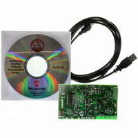
Manufacturer Part Number
TMPSNS-RTD1
Description
BOARD EVAL PT100 RTD TEMP SENSOR
Manufacturer
Microchip Technology
Datasheets
1.MCP3301-CIMS.pdf
(32 pages)
2.PCM18XR1.pdf
(438 pages)
3.MCP6S22DM-PICTL.pdf
(43 pages)
4.TMPSNS-RTD1.pdf
(26 pages)
Specifications of TMPSNS-RTD1
Sensor Type
Temperature
Interface
USB
Embedded
Yes, MCU, 8-Bit
Utilized Ic / Part
MCP3301, MCP6S26, PIC18F2550
Processor To Be Evaluated
MCP6S26, MCP3301, MCP6024, MCP41010, PIC18F2550, TC1071, MCP6002
Data Bus Width
12 bit
Interface Type
USB
Lead Free Status / RoHS Status
Not applicable / Not applicable
Voltage - Supply
-
Sensitivity
-
Sensing Range
-
Lead Free Status / RoHS Status
Lead free / RoHS Compliant, Not applicable / Not applicable


MCP3301
ELECTRICAL SPECIFICATIONS (CONTINUED)
DS21700C-page 4
Electrical Characteristics: Unless otherwise noted, all parameters apply at V
configuration (Figure 3-4) with fixed common mode voltage of 2.5V. All parameters apply over temperature with
T
Reference Input
Voltage Range
Current Drain
Analog Inputs
Full-Scale Input Span
Absolute Input Voltage
Leakage Current
Switch Resistance
Sample Capacitor
Digital Input/Output
Data Coding Format
High Level Input Voltage
Low Level Input Voltage
High Level Output Voltage
Low Level Output Voltage
Input Leakage Current
Output Leakage Current
Pin Capacitance
Timing Specifications
Clock Frequency (Note 8)
Clock High Time
Clock Low Time
CS Fall To First Rising CLK Edge
CLK Fall To Output Data Valid
CLK Fall To Output Enable
CS Rise To Output Disable
CS Disable Time
D
D
Note 1: This specification is established by characterization and not 100% tested.
AMB
OUT
OUT
= -40°C to +85°C (Note 7). Conversion speed (f
Rise Time
Fall Time
2: See characterization graphs that relate converter performance to V
3: V
4: V
5: Maximum clock frequency specification must be met.
6: V
7: MSOP devices are only specified at 25°C and +85°C.
8: For slow sample rates, see Section 6.2.1 for limitations on clock frequency.
REF
IN
DD
Parameter
= 0.1V to 4.9V @ 1 kHz.
= 5VDC ±500 mV
= 400 mV, V
IN
= 0.1V to 4.9V @ 1 kHz
P
-
P
@ 1 kHz, see test circuit Figure 3-3.
IN(+)-IN(-)
C
Symbol
C
IN
IN(+)
IN(-)
t
SAMPLE
V
f
SUCS
t
V
V
, C
t
t
R
V
I
t
t
CSH
CLK
t
I
DIS
t
t
DO
EN
LO
LO
OH
HI
R
OL
LI
F
IH
IL
S
OUT
0.7 V
SAMPLE)
0.085
0.085
-V
Min
-0.3
-0.3
275
275
100
580
Binary Two’s Complement
0.4
4.1
-10
-10
—
—
—
—
—
—
—
—
—
—
—
—
—
REF
DD
is 100 ksps with f
0.001
0.001
Typ
100
25
—
—
—
—
—
—
—
—
—
—
—
—
—
—
—
—
—
—
—
—
—
—
1
V
V
0.3 V
DD
DD
Max
V
0.85
V
150
125
200
125
200
100
100
100
0.4
1.7
±1
10
10
10
—
—
—
—
—
—
—
—
3
REF
DD
+ 0.3
+ 0.3
DD
REF
CLK
DD
= 5V, V
level.
= 17*f
Units
MHz
MHz
SS
SAMPLE
µA
µA
µA
kΩ
µA
µA
pF
pF
ns
ns
ns
ns
ns
ns
ns
ns
ns
ns
ns
V
V
V
V
V
V
V
V
= 0V, and V
Note 2
CS = V
See Figure 6-3
See Figure 6-3
I
I
V
V
T
V
V
Note 5
Note 5
V
V
V
V
See test circuits, Figure 3-1
(Note 1)
See test circuits, Figure 3-1; Note 1
See test circuits, Figure 3-1; Note 1
OH
OL
AMB
IN
OUT
DD
DD
DD
DD
DD
DD
© 2007 Microchip Technology Inc.
= 1 mA, V
= -1 mA, V
= V
= 5V, f
= 2.7V, f
= 5V, see Figure 3-1
= 2.7V, see Figure 3-1
= 5V, see Figure 3-1
= 2.7V, see Figure 3-1
= 25°C, f = 1 MHz, Note 1
= V
REF
SS
DD
SS
= 5V. Full differential input
or V
= 5V
SAMPLE
or V
Conditions
SAMPLE
DD
DD
DD
DD
= 4.5V
= 4.5V
= 100 ksps
= 50 ksps
Related parts for TMPSNS-RTD1
Image
Part Number
Description
Manufacturer
Datasheet
Request
R

Part Number:
Description:
Manufacturer:
Microchip Technology Inc.
Datasheet:
Part Number:
Description:
Manufacturer:
Microchip Technology Inc.
Datasheet:
Part Number:
Description:
Manufacturer:
Microchip Technology Inc.
Datasheet:
Part Number:
Description:
Manufacturer:
Microchip Technology Inc.
Datasheet:
Part Number:
Description:
Manufacturer:
Microchip Technology Inc.
Datasheet:
Part Number:
Description:
Manufacturer:
Microchip Technology Inc.
Datasheet:
Part Number:
Description:
Manufacturer:
Microchip Technology Inc.
Datasheet:
Part Number:
Description:
Manufacturer:
Microchip Technology Inc.
Datasheet: