TMPSNS-RTD1 Microchip Technology, TMPSNS-RTD1 Datasheet - Page 22
TMPSNS-RTD1
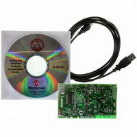
Manufacturer Part Number
TMPSNS-RTD1
Description
BOARD EVAL PT100 RTD TEMP SENSOR
Manufacturer
Microchip Technology
Datasheets
1.MCP3301-CIMS.pdf
(32 pages)
2.PCM18XR1.pdf
(438 pages)
3.MCP6S22DM-PICTL.pdf
(43 pages)
4.TMPSNS-RTD1.pdf
(26 pages)
Specifications of TMPSNS-RTD1
Sensor Type
Temperature
Interface
USB
Embedded
Yes, MCU, 8-Bit
Utilized Ic / Part
MCP3301, MCP6S26, PIC18F2550
Processor To Be Evaluated
MCP6S26, MCP3301, MCP6024, MCP41010, PIC18F2550, TC1071, MCP6002
Data Bus Width
12 bit
Interface Type
USB
Lead Free Status / RoHS Status
Not applicable / Not applicable
Voltage - Supply
-
Sensitivity
-
Sensing Range
-
Lead Free Status / RoHS Status
Lead free / RoHS Compliant, Not applicable / Not applicable


MCP3301
7.3
With most microcontroller SPI ports, it is required to
clock out eight bits at a time. Using a hardware SPI port
with the MCP3301 is very easy because each conver-
sion requires 16 clocks. For example, Figure 7-4 and
Figure 7-5 show how the MCP3301 can be interfaced
to a microcontroller with a standard SPI port. Since the
MCP3301 always clocks data out on the falling edge of
clock, the MCU SPI port must be configured to match
this operation. SPI Mode 0,0 (clock idles low) and SPI
Mode 1,1 (clock idles high) are both compatible with
the MCP3301. Figure 7-4 depicts the operation shown
in SPI Mode 0,0, which requires that the CLK from the
microcontroller idles in the ‘low’ state. As shown in the
diagram, the sign bit is clocked out of the ADC on the
FIGURE 7-4:
(Mode 0,0: SCLK idles low).
FIGURE 7-5:
(Mode 1,1: SCLK idles high).
DS21700C-page 22
D
D
CLK
CLK
CS
CS
OUT
OUT
Using the MCP3301 with
Microcontroller (MCU) SPI Ports
HI-Z
HI-Z
?
?
1
1
Data stored into MCU receive register
after transmission of first 8 bits
Data stored into MCU receive register
after transmission of first 8 bits
?
?
2
2
NULL
NULL
BIT SB B11 B10
BIT SB
0
0
SPI Communication with the MCP3301 using 8-bit segments
SPI Communication with the MCP3301 using 8-bit segments
3
3
SB
SB
4
4
B11 B10 B9
B11 B10 B9
B11 B10 B9
5
5
6
6
B9
7
7
B8
B8
B8
8
B8
8
B7
B7
B7
B7
Data stored into MCU receive register
after transmission of second 8 bits
Data stored into MCU receive register
after transmission of second 8 bits
9
9
B6
B6
B6
B6
10
10
B5
B5
B5
B5
11
11
B4
B4
falling edge of the third clock pulse, followed by the
remaining 12 data bits (MSB first). Once the first eight
clocks have been sent to the device, the microcontrol-
ler’s receive buffer will contain two unknown bits (for
the first two clocks, the output is high impedance), fol-
lowed by the null bit, the sign bit and the highest order
four bits of the conversion. After the second eight
clocks have been sent to the device, the MCU receive
register will contain the lowest order 8 data bits. Notice
that, on the falling edge of clock 16, the ADC has begun
to shift out LSB first data.
Figure 7-5 shows the same scenario in SPI Mode 1,1,
which requires that the clock idles in the high state. As
with mode 0,0, the ADC outputs data on the falling
edge of the clock and the MCU latches data from the
ADC in on the rising edge of the clock.
B4
B4
12
12
B3
B3
B3
B3
13
13
B2
B2
B2
B2
14
14
B1
B1
B1
B1
15
15
B0
B0
B0
16
16
B0
B1
HI-Z
HI-Z
© 2007 Microchip Technology Inc.
LSB first data begins
to come out
LSB first data begins
to come out
MCU latches data from ADC
on rising edges of SCLK
MCU latches data from ADC
on rising edges of SCLK
Data is clocked out of
ADC on falling edges
Data is clocked out of
ADC on falling edges
X = Don’t Care Bits
? = Unknown Bits
X = Don’t Care Bits
? = Unknown Bits
Related parts for TMPSNS-RTD1
Image
Part Number
Description
Manufacturer
Datasheet
Request
R

Part Number:
Description:
Manufacturer:
Microchip Technology Inc.
Datasheet:
Part Number:
Description:
Manufacturer:
Microchip Technology Inc.
Datasheet:
Part Number:
Description:
Manufacturer:
Microchip Technology Inc.
Datasheet:
Part Number:
Description:
Manufacturer:
Microchip Technology Inc.
Datasheet:
Part Number:
Description:
Manufacturer:
Microchip Technology Inc.
Datasheet:
Part Number:
Description:
Manufacturer:
Microchip Technology Inc.
Datasheet:
Part Number:
Description:
Manufacturer:
Microchip Technology Inc.
Datasheet:
Part Number:
Description:
Manufacturer:
Microchip Technology Inc.
Datasheet: