TMPSNS-RTD1 Microchip Technology, TMPSNS-RTD1 Datasheet - Page 21
TMPSNS-RTD1
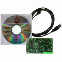
Manufacturer Part Number
TMPSNS-RTD1
Description
BOARD EVAL PT100 RTD TEMP SENSOR
Manufacturer
Microchip Technology
Datasheets
1.MCP3301-CIMS.pdf
(32 pages)
2.PCM18XR1.pdf
(438 pages)
3.MCP6S22DM-PICTL.pdf
(43 pages)
4.TMPSNS-RTD1.pdf
(26 pages)
Specifications of TMPSNS-RTD1
Sensor Type
Temperature
Interface
USB
Embedded
Yes, MCU, 8-Bit
Utilized Ic / Part
MCP3301, MCP6S26, PIC18F2550
Processor To Be Evaluated
MCP6S26, MCP3301, MCP6024, MCP41010, PIC18F2550, TC1071, MCP6002
Data Bus Width
12 bit
Interface Type
USB
Lead Free Status / RoHS Status
Not applicable / Not applicable
Voltage - Supply
-
Sensitivity
-
Sensing Range
-
Lead Free Status / RoHS Status
Lead free / RoHS Compliant, Not applicable / Not applicable


7.2
Communication with the device is completed using a
standard SPI compatible serial interface. Initiating com-
munication with the MCP3301 begins with the CS
going low. If the device was powered up with the CS pin
low, it must be brought high and back low to initiate
communication. The device will begin to sample the
analog input on the first rising edge of CLK after CS
goes low. The sample period will end in the falling edge
of the second clock, at which time the device will output
a low null bit. The next 13 clocks will output the result
of the conversion with the sign bit first, followed by the
FIGURE 7-2:
FIGURE 7-3:
© 2007 Microchip Technology Inc.
CLK
D
CS
D
OUT
CS
CLK
OUT
t
ACQ
Communicating with the MCP3301
* After completing the data transfer, if further clocks are applied with CS low, the ADC will output LSB first data,
followed by zeros indefinitely. See Figure 7-2 below.
** t
high impedance node, leaving the CLK running to clock out the LSB-first data or zeros.
HI-Z
HI-Z
high impedance node, leaving the CLK running to clock out the LSB-first data or zeros.
DATA
* After completing the data transfer, if further clocks are applied with CS low, the ADC will output zeros indefi-
nitely.
** t
DATA
t
t
ACQ
SUCS
: during this time, the bias current and the comparator power down and the reference input becomes a
t
NULL
SUCS
: during this time, the bias current and the comparator power down and the reference input becomes a
BIT
Communication with MCP3301 (MSB first Format).
Communication with MCP3301 (LSB first Format).
NULL
SB
BIT
B11 B10
SB
B11 B10 B9
B9
B8
t
CONV
B7
B6
B8
B5
t
SAMPLE
B7
t
CONV
B4
B6
B3
B2
B5
B1
t
B4
SAMPLE
12 remaining data bits, as shown in Figure 7-2. Data is
always output from the device on the falling edge of the
clock. If all 13 data bits have been transmitted and the
device continues to receive clocks while the CS is held
low, the device will output the conversion result LSB
first, as shown in Figure 7-3. If more clocks are pro-
vided to the device while CS is still low (after the LSB
first data has been transmitted), the device will clock
out zeros indefinitely.
B0
B3
B1
B2
B2
B3
B1 B0
t
CSH
B4
B5
*
t
DATA
t
Power Down
DATA
B6
**
**
Power
Down
HI-Z
B7
B8
MCP3301
B9 B10
NULL
BIT
SB B11 B10 B9
B11
DS21700C-page 21
t
CSH
SB
*
HI-Z
Related parts for TMPSNS-RTD1
Image
Part Number
Description
Manufacturer
Datasheet
Request
R

Part Number:
Description:
Manufacturer:
Microchip Technology Inc.
Datasheet:
Part Number:
Description:
Manufacturer:
Microchip Technology Inc.
Datasheet:
Part Number:
Description:
Manufacturer:
Microchip Technology Inc.
Datasheet:
Part Number:
Description:
Manufacturer:
Microchip Technology Inc.
Datasheet:
Part Number:
Description:
Manufacturer:
Microchip Technology Inc.
Datasheet:
Part Number:
Description:
Manufacturer:
Microchip Technology Inc.
Datasheet:
Part Number:
Description:
Manufacturer:
Microchip Technology Inc.
Datasheet:
Part Number:
Description:
Manufacturer:
Microchip Technology Inc.
Datasheet: