TMPSNS-RTD1 Microchip Technology, TMPSNS-RTD1 Datasheet - Page 17
TMPSNS-RTD1
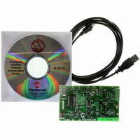
Manufacturer Part Number
TMPSNS-RTD1
Description
BOARD EVAL PT100 RTD TEMP SENSOR
Manufacturer
Microchip Technology
Datasheets
1.MCP3301-CIMS.pdf
(32 pages)
2.PCM18XR1.pdf
(438 pages)
3.MCP6S22DM-PICTL.pdf
(43 pages)
4.TMPSNS-RTD1.pdf
(26 pages)
Specifications of TMPSNS-RTD1
Sensor Type
Temperature
Interface
USB
Embedded
Yes, MCU, 8-Bit
Utilized Ic / Part
MCP3301, MCP6S26, PIC18F2550
Processor To Be Evaluated
MCP6S26, MCP3301, MCP6024, MCP41010, PIC18F2550, TC1071, MCP6002
Data Bus Width
12 bit
Interface Type
USB
Lead Free Status / RoHS Status
Not applicable / Not applicable
Voltage - Supply
-
Sensitivity
-
Sensing Range
-
Lead Free Status / RoHS Status
Lead free / RoHS Compliant, Not applicable / Not applicable


FIGURE 6-3:
6.2.1
When the MCP3301 initiates, charge is stored on the
sample capacitor. When the sample period is complete,
the device converts one bit for each clock that is
received. It is important for the user to note that a slow
clock rate will allow charge to bleed off the sample
capacitor while the conversion is taking place. For the
MCP330X devices, the recommended minimum clock
speed during the conversion cycle (t
Failure to meet this criteria may introduce linearity
errors into the conversion outside the rated specifica-
tions. It should be noted that, during the entire conver-
sion cycle, the A/D converter does not have
requirements for clock speed or duty cycle as long as
all timing specifications are met.
6.3
For pseudo-differential bipolar operation, the biasing
circuit shown in Figure 6-4 shows a single-ended input
AC coupled to the converter. This configuration will give
a digital output range of -4096 to +4095. With the 2.5V
reference, the LSB size is equal to 610 µV.
Although the ADC is not production tested with a 2.5V
reference as shown, linearity will not change more than
0.1 LSB. See Figure 2-2 and 2-9 for DNL and INL
errors versus V
between the high pass corner and the acquisition time.
The value of C will need to be quite large in order to
bring down the high pass corner. The value of R needs
to be 1 kΩ or less, since higher input impedances
© 2007 Microchip Technology Inc.
Legend
VA
C
I
leakage
sample
CHx
C
Biasing Solutions
R
R
SS
VA
pin
R
ss
V
SS
s
MAINTAINING MINIMUM CLOCK
SPEED
t
=
=
=
=
=
=
=
=
=
CHx
REF
signal source
source impedance
input channel pad
input pin capacitance
threshold voltage
leakage current at the pin
due to various junctions
sampling switch
sampling switch resistor
sample/hold capacitance
at V
Analog Input Model.
DD
= 5V. A trade-off exists
7 pF
C
PIN
CONV
V
DD
V
V
) is 85 kHz.
T
T
= 0.6V
= 0.6V
I
±1 nA
LEAKAGE
require additional acquisition time. Using the values in
Figure 6-4, we have a 100 Hz corner frequency. See
Figure 2-12 for the relationship between input imped-
ance and acquisition time.
FIGURE 6-4:
circuit for bipolar operation.
Using an external operational amplifier on the input
allows for gain and buffers the input signal from the
input to the ADC, allowing for a higher source
impedance. This circuit is shown in Figure 6-5.
V
IN
10 µF C
SS
1 k
1 µF
Sampling
Switch
Ω
R
Ρ
S
V
= 1 kΩ
Pseudo-differential biasing
IN+
IN-
OUT
MCP1525
V
MCP3301
MCP3301
SS
V
C
= DAC capacitance
= 25 pF
IN
SAMPLE
0.1 µF
V
REF
DS21700C-page 17
V
DD
0.1 µF
= 5V
Related parts for TMPSNS-RTD1
Image
Part Number
Description
Manufacturer
Datasheet
Request
R

Part Number:
Description:
Manufacturer:
Microchip Technology Inc.
Datasheet:
Part Number:
Description:
Manufacturer:
Microchip Technology Inc.
Datasheet:
Part Number:
Description:
Manufacturer:
Microchip Technology Inc.
Datasheet:
Part Number:
Description:
Manufacturer:
Microchip Technology Inc.
Datasheet:
Part Number:
Description:
Manufacturer:
Microchip Technology Inc.
Datasheet:
Part Number:
Description:
Manufacturer:
Microchip Technology Inc.
Datasheet:
Part Number:
Description:
Manufacturer:
Microchip Technology Inc.
Datasheet:
Part Number:
Description:
Manufacturer:
Microchip Technology Inc.
Datasheet: