TMPSNS-RTD1 Microchip Technology, TMPSNS-RTD1 Datasheet - Page 19
TMPSNS-RTD1
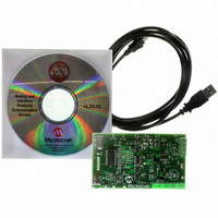
Manufacturer Part Number
TMPSNS-RTD1
Description
BOARD EVAL PT100 RTD TEMP SENSOR
Manufacturer
Microchip Technology
Datasheets
1.MCP3301-CIMS.pdf
(32 pages)
2.PCM18XR1.pdf
(438 pages)
3.MCP6S22DM-PICTL.pdf
(43 pages)
4.TMPSNS-RTD1.pdf
(26 pages)
Specifications of TMPSNS-RTD1
Sensor Type
Temperature
Interface
USB
Embedded
Yes, MCU, 8-Bit
Utilized Ic / Part
MCP3301, MCP6S26, PIC18F2550
Processor To Be Evaluated
MCP6S26, MCP3301, MCP6024, MCP41010, PIC18F2550, TC1071, MCP6002
Data Bus Width
12 bit
Interface Type
USB
Lead Free Status / RoHS Status
Not applicable / Not applicable
Voltage - Supply
-
Sensitivity
-
Sensing Range
-
Lead Free Status / RoHS Status
Lead free / RoHS Compliant, Not applicable / Not applicable


6.5
Inaccurate conversion results may occur if the signal
source for the A/D converter is not a low impedance
source. Buffering the input will solve the impedance
issue. It is also recommended that an analog filter be
used to eliminate any signals that may be aliased back
into the conversion results. Using an op amp to drive
the analog input of the MCP3301 is illustrated in
Figure 6-9. This amplifier provides a low impedance
source for the converter input and low pass filter, which
eliminates unwanted high frequency noise. Values
shown are for a 10 Hz Butterworth Low pass filter.
Low pass (anti-aliasing) filters can be designed using
Microchip’s interactive FilterLab
will calculate capacitor and resistor values as well as
determine the number of poles that are required for the
application. For more information on filtering signals,
see AN-699 “Anti-Aliasing Analog Filters for Data
Acquisition Systems”.
FIGURE 6-9:
Amplifier is used to implement a 2nd order anti-
aliasing filter for the signal being converted by
the MCP3301.
© 2007 Microchip Technology Inc.
V
IN
7.86 kΩ
14.6 kΩ
0.1 µF
Buffering/Filtering the Analog
Inputs
1 µF
2.2 µF
Reference
4.096V
MCP1541
MCP601
+
-
The MCP601 Operational
C
L
1 µF
®
IN+
software. FilterLab
IN-
MCP3301
V
REF
V
DD
10 µF
0.1 µF
6.6
When laying out a printed circuit board for use with
analog components, care should be taken to reduce
noise wherever possible. A bypass capacitor from V
to ground should always be used with this device and
should be placed as close as possible to the device pin.
A bypass capacitor value of 0.1 µF is recommended.
Digital and analog traces should be separated as much
as possible on the board with no traces running under-
neath the device or bypass capacitor. Extra precau-
tions should be taken to keep traces with high
frequency signals (such as clock lines) as far as
possible from analog traces.
Use of an analog ground plane is recommended in
order to keep the ground potential the same for all
devices on the board. Providing V
devices in a “star” configuration can also reduce noise
by eliminating current return paths and associated
errors (Figure 6-10). For more information on layout
tips when using the MCP3301 or other ADC devices,
refer to AN-688 “Layout Tips for 12-Bit A/D Converter
Applications”.
FIGURE 6-10:
‘Star’ configuration in order to reduce errors
caused by current return paths.
Device 1
Layout Considerations
Device 2
Connection
V
DD
V
DD
traces arranged in a
MCP3301
Device 3
DD
DS21700C-page 19
connections to
Device 4
DD
Related parts for TMPSNS-RTD1
Image
Part Number
Description
Manufacturer
Datasheet
Request
R

Part Number:
Description:
Manufacturer:
Microchip Technology Inc.
Datasheet:
Part Number:
Description:
Manufacturer:
Microchip Technology Inc.
Datasheet:
Part Number:
Description:
Manufacturer:
Microchip Technology Inc.
Datasheet:
Part Number:
Description:
Manufacturer:
Microchip Technology Inc.
Datasheet:
Part Number:
Description:
Manufacturer:
Microchip Technology Inc.
Datasheet:
Part Number:
Description:
Manufacturer:
Microchip Technology Inc.
Datasheet:
Part Number:
Description:
Manufacturer:
Microchip Technology Inc.
Datasheet:
Part Number:
Description:
Manufacturer:
Microchip Technology Inc.
Datasheet: