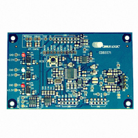
CDB5571 Cirrus Logic Inc, CDB5571 Datasheet - Page 8
CDB5571
Manufacturer Part Number
CDB5571
Description
DEV BOARD FOR CS5571 W/MUX
Manufacturer
Cirrus Logic Inc
Type
A/Dr
Specifications of CDB5571
Number Of Adc's
1
Number Of Bits
16
Sampling Rate (per Second)
100k
Data Interface
Serial
Inputs Per Adc
2 Single
Input Range
2.4 ~ 4.2 V
Voltage Supply Source
Dual ±
Operating Temperature
-40°C ~ 85°C
Utilized Ic / Part
CS5571
Product
Data Conversion Development Tools
Conversion Rate
100 KSPS
Resolution
16 bit
Maximum Clock Frequency
16 MHz
Interface Type
SPI
Supply Voltage (max)
3.3 V
Supply Voltage (min)
- 2.5 V
For Use With/related Products
CS5571
Lead Free Status / RoHS Status
Contains lead / RoHS non-compliant
Lead Free Status / RoHS Status
Lead free / RoHS Compliant, Contains lead / RoHS non-compliant
Other names
598-1275
CDB5571-1
CDB5571-1


SWITCHING CHARACTERISTICS
T
VL - VLR = 3.3 V, ±5%, 2.5 V, ±5%, or 1.8 V, ±5%
Input levels: Logic 0 = 0V = Low; Logic 1 = VD+ = High; CL = 15 pF.
8
Serial Port Timing in SSC Mode (SMODE = VL)
Data hold time after SCLK rising
Serial Clock (Out)
(Note 14, 15)
RDY rising after last SCLK rising
CS falling to MSB stable
First SCLK rising after CS falling
CS hold time (low) after SCLK rising
SCLK, SDO tri-state after CS rising
SCLK(o)
A
MCLK
= -40 to +85 °C; V1+ = V2+ = +2.5 V, ±5%; V1- = V2- = -2.5 V, ±5%;
SDO
RDY
CS
14. SDO and SCLK will be high impedance when CS is high. In some systems SCLK and SDO may require pull-down
15. SCLK = MCLK/2.
resistors.
Figure 2. SSC Mode - Read Timing, CS falling after RDY falls (Not to Scale)
t
11
Parameter
t
12
MSB
MSB–1
Pulse Width (high)
Pulse Width (low)
t
(CONTINUED)
7
3/25/08
10:56
t
Symbol
8
t
t
t
t
t
t
t
t
10
12
13
14
11
7
8
9
t
9
Min
50
50
10
-
-
-
-
-
LSB+1
t
13
LSB
Typ
10
10
8
8
5
-
-
-
t
14
t
10
Max
-
-
-
-
-
-
-
-
CS5571
DS768PP1
MCLKs
MCLKs
Unit
ns
ns
ns
ns
ns
ns
Related parts for CDB5571
Image
Part Number
Description
Manufacturer
Datasheet
Request
R

Part Number:
Description:
Development Kit
Manufacturer:
Cirrus Logic Inc
Datasheet:
Part Number:
Description:
Development Kit
Manufacturer:
Cirrus Logic Inc
Datasheet:


Part Number:
Description:
High-efficiency PFC + Fluorescent Lamp Driver Reference Design
Manufacturer:
Cirrus Logic Inc
Datasheet:
Part Number:
Description:
Development Kit
Manufacturer:
Cirrus Logic Inc
Datasheet:
Part Number:
Description:
Development Kit
Manufacturer:
Cirrus Logic Inc
Datasheet:

Part Number:
Description:
Development Kit
Manufacturer:
Cirrus Logic Inc
Datasheet:
Part Number:
Description:
Development Kit
Manufacturer:
Cirrus Logic Inc
Datasheet:
Part Number:
Description:
Development Kit
Manufacturer:
Cirrus Logic Inc
Datasheet:
Part Number:
Description:
Development Kit
Manufacturer:
Cirrus Logic Inc
Datasheet:

Part Number:
Description:
EVALUATION BOARD FOR CS8427
Manufacturer:
Cirrus Logic Inc
Datasheet:

Part Number:
Description:
BOARD EVAL FOR CS8416 RCVR
Manufacturer:
Cirrus Logic Inc
Datasheet:

Part Number:
Description:
EVALUATION BOARD FOR CS8420
Manufacturer:
Cirrus Logic Inc
Datasheet:

Part Number:
Description:
KIT DEVELOPMENT EP9315 ARM9
Manufacturer:
Cirrus Logic Inc
Datasheet:

Part Number:
Description:
KIT DEVELOPMENT EP9302 ARM9
Manufacturer:
Cirrus Logic Inc
Datasheet: