CDB5571 Cirrus Logic Inc, CDB5571 Datasheet - Page 27
CDB5571
Manufacturer Part Number
CDB5571
Description
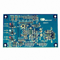
DEV BOARD FOR CS5571 W/MUX
Manufacturer
Cirrus Logic Inc
Type
A/Dr
Specifications of CDB5571
Number Of Adc's
1
Number Of Bits
16
Sampling Rate (per Second)
100k
Data Interface
Serial
Inputs Per Adc
2 Single
Input Range
2.4 ~ 4.2 V
Voltage Supply Source
Dual ±
Operating Temperature
-40°C ~ 85°C
Utilized Ic / Part
CS5571
Product
Data Conversion Development Tools
Conversion Rate
100 KSPS
Resolution
16 bit
Maximum Clock Frequency
16 MHz
Interface Type
SPI
Supply Voltage (max)
3.3 V
Supply Voltage (min)
- 2.5 V
For Use With/related Products
CS5571
Lead Free Status / RoHS Status
Contains lead / RoHS non-compliant
Lead Free Status / RoHS Status
Lead free / RoHS Compliant, Contains lead / RoHS non-compliant
Other names
598-1275
CDB5571-1
CDB5571-1


3.13 Using the CS5571 in Multiplexing Applications
The CS5571 is a delta-sigma A/D converter. Delta-sigma converters use oversampling as means to
achieve high signal-to-noise performance. This means that once a conversion is started, the converter
takes many samples to compute the resulting output word. The analog input for the signal to be converted
must remain active during the entire conversion until RDY falls.
The CS5571 can be used in multiplexing applications, but the system timing for changing the multiplexer
channel and for starting a new conversion will depend upon the multiplexer system architecture.
The simplest system is illustrated in
presented to the converter must fully settle. After the signal has settled, the CONV signal is issued to the
converter to start a conversion. Being a delta-sigma converter, the signal must remain present at the input
of the converter until the conversion is completed. Once the conversion is completed, RDY falls. At this
time the multiplexer can be changed to the next channel and the data can be read from the serial port.
The CONV signal should be delayed until after the data is read and until the new analog signal has settled.
In this configuration, the throughput of the converter will be dictated by the settling time of the analog input
circuit and the conversion time of the converter. The conversion data can be read from the serial port after
the multiplexer is changed to the new channel while the analog input signal is settling.
A more complex multiplexing scheme can be used to increase the throughput of the converter is illustrated
in
DS768PP1
Figure
28. In this circuit, two banks of multiplexers are used.
Advance
CONV
Mux
RDY
CH1
CH2
CH3
CH4
Figure 27. Simple Multiplexing Scheme
Figure
27. Any time the multiplexer is changed, the analog signal
CH1
3/25/08
Settling Time
10:56
Amplifier
150pF
90
2k
4700pF
Throughput
C0G
Conversion Time
AIN
ACOM
CS5571
CH2
Settling Time
Amplifier
CS5571
27
Related parts for CDB5571
Image
Part Number
Description
Manufacturer
Datasheet
Request
R

Part Number:
Description:
Development Kit
Manufacturer:
Cirrus Logic Inc
Datasheet:
Part Number:
Description:
Development Kit
Manufacturer:
Cirrus Logic Inc
Datasheet:


Part Number:
Description:
High-efficiency PFC + Fluorescent Lamp Driver Reference Design
Manufacturer:
Cirrus Logic Inc
Datasheet:
Part Number:
Description:
Development Kit
Manufacturer:
Cirrus Logic Inc
Datasheet:
Part Number:
Description:
Development Kit
Manufacturer:
Cirrus Logic Inc
Datasheet:

Part Number:
Description:
Development Kit
Manufacturer:
Cirrus Logic Inc
Datasheet:
Part Number:
Description:
Development Kit
Manufacturer:
Cirrus Logic Inc
Datasheet:
Part Number:
Description:
Development Kit
Manufacturer:
Cirrus Logic Inc
Datasheet:
Part Number:
Description:
Development Kit
Manufacturer:
Cirrus Logic Inc
Datasheet:

Part Number:
Description:
EVALUATION BOARD FOR CS8427
Manufacturer:
Cirrus Logic Inc
Datasheet:

Part Number:
Description:
BOARD EVAL FOR CS8416 RCVR
Manufacturer:
Cirrus Logic Inc
Datasheet:

Part Number:
Description:
EVALUATION BOARD FOR CS8420
Manufacturer:
Cirrus Logic Inc
Datasheet:

Part Number:
Description:
KIT DEVELOPMENT EP9315 ARM9
Manufacturer:
Cirrus Logic Inc
Datasheet:

Part Number:
Description:
KIT DEVELOPMENT EP9302 ARM9
Manufacturer:
Cirrus Logic Inc
Datasheet: