MT18HVF6472Y-53EB1 Micron Technology Inc, MT18HVF6472Y-53EB1 Datasheet
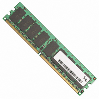
MT18HVF6472Y-53EB1
Specifications of MT18HVF6472Y-53EB1


Related parts for MT18HVF6472Y-53EB1


MT18HVF6472Y-53EB1 Summary of contents
Page 1
DDR2 VLP Registered DIMM (RDIMM) MT18HVF12872(P) – 1GB For the latest data sheet and for component data sheets, refer to Micron's Web site: Features • Supports 95 C with double refresh ° • Fits with the ATCA form factor • ...
Page 2
Figure 2: Module Part Numbers MT Micron Technology Number of DRAM Process Technology H 1.8V (DDR2 SDRAM) Product Family TF DDR2 FBGA TS DDR2 DDP (Dual die in package) TD DDR2 flip chip TJ DDR2 CSP stack VF DDR2 VLP ...
Page 3
Pin Assignments and Descriptions Table 4: Pin Assignment 240-Pin RDIMM Front Pin Symbol Pin Symbol Pin Symbol DQ19 61 REF DQ0 33 DQ24 63 4 DQ1 34 DQ25 64 ...
Page 4
Table 5: Pin Descriptions Refer to Table 4 on page 3 for more information Symbol Type Source ODT0 Input Register (SSTL18) CK0, CK0# Input (SSTL18) CKE0 Input Register (SSTL18) S0# Input Register (SSTL18) RAS#, CAS#, Input Register WE# (SSTL18) BA0, ...
Page 5
Table 5: Pin Descriptions (continued) Refer to Table 4 on page 3 for more information Symbol Type Source V Supply DRAM, REF Register V Supply SS V Supply DDSPD NC – RFU – PDF: 09005aef82255aba/Source: 09005aef82255a83 HVF18C64_128_256x72G.fm - Rev. B ...
Page 6
Functional Block Diagram Figure 3: Functional Block Diagram V SS RS0# DQS0 DQS0# DQS1 DQS1# DQS2 DQS2# DQS3 DQS3# DQS4 DQS4# DQS5# DQS6 DQS6# DQS7 DQS7# DQS8 DQS8# U16 S0# RS0#: DDR2 SDRAMs R BA0–BA1 RBA0 – RBA1: DDR2 SDRAMs ...
Page 7
... READs and by the memory controller during WRITEs. DQS is edge- aligned with data for READs and center-aligned with data for WRITEs. DDR2 SDRAM modules operate from a differential clock (CK and CK#); the crossing of CK going HIGH and CK# going LOW will be referred to as the positive edge of CK. Input data is registered on both edges of DQS, and output data is referenced to both edges of DQS, as well as to both edges of CK ...
Page 8
... When inductance and delay parameters associated with trace lengths are used in simulations, they are significantly more accurate and real- istic than a gross estimation of module capacitance. Simulations can then render a considerably more accurate result. JEDEC modules are now designed by using simula- tions to close timing budgets. Table 7: ...
Page 9
I Specifications DD Table 8: DDR2 I Specifications and Conditions – 1GB DD Values shown for MT47H128M4 DDR2 SDRAM only and are computed from values specified in the 512Mb (128 Meg x 4) component data sheet Parameter/Condition Operating one bank ...
Page 10
Registers Table 9: Register ( uses SSTU32865 devices) Parameter Symbol DC high-level input voltage DC low-level input voltage high-level IH AC input voltage AC low-level V ...
Page 11
PLL Table 10: PLL (uses a 97U877B device) Parameter Symbol V DC high-level input voltage DC low-level input voltage V Input voltage (limits high-level input voltage low-level input voltage Input differential-pair cross V voltage Input ...
Page 12
Serial Presence-Detect Table 12: Serial Presence-Detect EEPROM DC Operating Conditions All voltages referenced to V Parameter/Condition Supply voltage Input high voltage: Logic 1; All inputs Input low voltage: Logic 0; All inputs Output low voltage 3mA OUT Input ...
Page 13
Table 14: Serial Presence-Detect Matrix “1”/“0”: serial data, “driven to HIGH”/“driven to LOW” Byte 0 Number of SPD bytes used by Micron 1 Total number of bytes in SPD device 2 Fundamental memory type 3 Number of row addresses on ...
Page 14
Table 14: Serial Presence-Detect Matrix (continued) “1”/“0”: serial data, “driven to HIGH”/“driven to LOW” Byte 32 Address and command setup time, 33 Address and command hold time, 34 Data/data mask input setup time, 35 Data/data mask input hold time, t ...
Page 15
Module Dimensions Figure 4: 240-Pin DDR2 DIMM 2.00 (0.079) R (4X 2.50 (0.098) D (2X) 2.30 (0.091) TYP PIN 1 1.0 (0.039) 1.0 (0.039) TYP TYP U12 U13 U14 3.05 (0.012) TYP PIN 240 2.20 (0.087) TYP ...