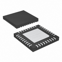
MAX8720ETX+ Maxim Integrated Products, MAX8720ETX+ Datasheet - Page 27

MAX8720ETX+
Manufacturer Part Number
MAX8720ETX+
Description
IC CNTRL VID STP DWN 36-TQFN
Manufacturer
Maxim Integrated Products
Datasheet
1.MAX8720ETXT.pdf
(31 pages)
Specifications of MAX8720ETX+
Applications
Controller, CPU GPU
Voltage - Input
2 ~ 28 V
Number Of Outputs
1
Voltage - Output
0.28 ~ 1.85 V
Operating Temperature
0°C ~ 85°C
Mounting Type
Surface Mount
Package / Case
36-TQFN Exposed Pad
Output Voltage
0.275 V to 1.85 V
Input Voltage
2 V to 28 V
Mounting Style
SMD/SMT
Maximum Operating Temperature
+ 85 C
Minimum Operating Temperature
- 40 C
Lead Free Status / RoHS Status
Lead free / RoHS Compliant
where N is the number of high-side MOSFETs used for
one regulator, and Q
in the MOSFET’s data sheet. For example, assume the
IRF7821 n-channel MOSFET is used on the high side.
According to the manufacturer’s data sheet, a single
IRF7821 has a maximum gate charge of 14nC (V
5V). Using the above equation, the required boost
capacitance is:
Select the closest standard value. This example
requires a 0.1µF ceramic capacitor.
The output-voltage adjust range for continuous-conduc-
tion operation is restricted by the nonadjustable 500ns
(max) minimum off-time one-shot (375ns max at
1000kHz). For best dropout performance, use the slower
(200kHz) on-time settings. When working with low input
voltages, the duty-factor limit must be calculated using
worst-case values for on- and off-times. Manufacturing
tolerances and internal propagation delays introduce an
error to the TON K-factor. This error is greater at higher
frequencies (Table 3). Also, keep in mind that transient-
response performance of buck regulators operated
close to dropout is poor, and bulk output capacitance
must often be added (see the V
Design Procedure section).
The absolute point of dropout is when the inductor cur-
rent ramps down during the minimum off-time (∆I
as much as it ramps up during the on-time (∆I
ratio h = ∆I
slew the inductor current higher in response to
increased load, and must always be greater than 1. As
h approaches 1, the absolute minimum dropout point,
the inductor current is less able to increase during
each switching cycle and V
unless additional output capacitance is used.
A reasonable minimum value for h is 1.5, but this may
be adjusted up or down to allow tradeoffs between
V
voltage. For a given value of h, the minimum operating
voltage can be calculated as:
SAG
, output capacitance, and minimum operating
V
IN(MIN )
UP
/ ∆I
Applications Information
=
C
BST
______________________________________________________________________________________
DOWN
1−
V
GATE
OUT
t
=
OFF(MIN )
1 14
200
is an indicator of the ability to
×
+ V
is the gate charge specified
K
Dropout Performance
mV
nC
DIS
SAG
×h
=
0 07
SAG
.
Dynamically Adjustable 6-Bit VID
+V
greatly increases
µ
CHG
equation in the
F
− V
DIS
UP
DOWN
). The
GS
=
)
where V
the discharge and charge paths, respectively (see the
On-Time One-Shot (TON) section), t
Electrical Characteristics table, and K is taken from
Table 3. The absolute minimum input voltage is calcu-
lated with h = 1.
If the calculated V
minimum input voltage, then operating frequency must
be reduced or output capacitance added to obtain
an acceptable V
anticipated, calculate V
transient response.
Dropout Design Example:
V
f
K = 1.8µs, worst-case K = 1.58µs
t
V
h = 1.5
Calculating again with h = 1 gives the absolute limit
of dropout:
Therefore, V
very large output capacitance, and a practical input
voltage with reasonable output capacitance is 3.2V.
The MAX8720 can be used with a direct battery con-
nection (one stage) or can obtain power from a regulat-
ed 5V supply (two stage). Each approach has
advantages, and careful consideration should go into
the selection of the final design.
The one-stage approach offers smaller total inductor
size and fewer capacitors overall due to the reduced
demands on the 5V supply. The transient response of
the single stage is better due to the ability to ramp up
the inductor current faster. The total efficiency of a sin-
gle stage is better than the two-stage approach.
The two-stage approach allows flexible placement due
to smaller circuit size and reduced local power dissipa-
tion. The power supply can be placed closer to the
CPU for better regulation and lower I
board traces. Although the two-stage design has worse
transient response than the single stage, this can be
offset by the use of a voltage-positioned converter.
SW
OFF(MIN)
OUT
DIS
V
V
One-Stage (Battery Input) vs. Two-Stage
Step-Down Controller
= 550kHz
IN(MIN)
IN(MIN)
= V
= 1.6V
DIS
CHG
= 500ns
= (1.6V + 0.1V) / (1 - 0.5µs x 1.5 / 1.58µs)
= (1.6V + 0.1V) / (1 - 0.5µs x 1.0 / 1.58µs)
and V
IN
= 100mV
must be greater than 2.5V, even with
CHG
+ 0.1V - 0.1V = 3.2V
+ 0.1V - 0.1V = 2.5V
SAG
IN(MIN)
are the parasitic voltage drops in
. If operation near dropout is
SAG
(5V Input) Applications
is greater than the required
to be sure of adequate
OFF(MIN)
2
R losses from PC
is from the
27


