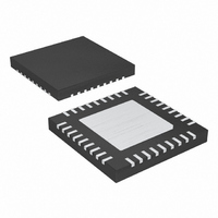
MAX8720ETX+ Maxim Integrated Products, MAX8720ETX+ Datasheet - Page 11

MAX8720ETX+
Manufacturer Part Number
MAX8720ETX+
Description
IC CNTRL VID STP DWN 36-TQFN
Manufacturer
Maxim Integrated Products
Datasheet
1.MAX8720ETXT.pdf
(31 pages)
Specifications of MAX8720ETX+
Applications
Controller, CPU GPU
Voltage - Input
2 ~ 28 V
Number Of Outputs
1
Voltage - Output
0.28 ~ 1.85 V
Operating Temperature
0°C ~ 85°C
Mounting Type
Surface Mount
Package / Case
36-TQFN Exposed Pad
Output Voltage
0.275 V to 1.85 V
Input Voltage
2 V to 28 V
Mounting Style
SMD/SMT
Maximum Operating Temperature
+ 85 C
Minimum Operating Temperature
- 40 C
Lead Free Status / RoHS Status
Lead free / RoHS Compliant
28 QSOP
13
14
15
16
17
18
19
20
21
22
23
24
25
26
27
28
—
—
—
PIN
6, 18, 28,
36 THIN
16, 17
30, 36
14,15
QFN
11
12
19
20
21
22
23
24
25
26
27
29
31
32
13
—
______________________________________________________________________________________
PGOOD
NAME
AGND
GNDS
PGND
GND
SKIP
SUS
N.C.
V
BST
DH
DL
D0
D5
D4
D3
D2
D1
LX
DD
Dynamically Adjustable 6-Bit VID
Ground Remote-Sense Input. For nonvoltage-positioned circuits, connect GNDS to
ground directly at the load. GNDS internally connects to the integrator that fine tunes the
output voltage. The output voltage rises by an amount of GNDS - AGND. For voltage-
positioned circuits, increase the output voltage by biasing GNDS with a resistor-divider
from REF to AGND.
Open-Drain Power-Good Output. PGOOD is normally high when the output is in
regulation. If V
low. During DAC code transitions, PGOOD is forced high for an additional 8 clocks after
the slew-rate controller finishes the transition. PGOOD is low during shutdown. PGOOD
upper threshold is blanked whenever the MAX8720 is in pulse-skipping mode (SKIP =
GND or SUS = high).
Analog and Power Ground. Also connects to the current-limit comparator.
Low-Side Gate-Driver Output. DL swings from PGND to V
Supply Voltage Input for the DL Gate Driver. Connect to the system supply voltage
(+4.5V to +5.5V). Bypass V
S usp end - M od e C ontr ol Inp ut. When S U S i s hi g h, the susp end - m od e V ID cod e, as
p r og r am m ed b y S 0 and S 1, i s d el i ver ed to the D AC . C onnect S U S to G N D i f the susp end -
m od e m ul ti p l exer i s not used . P GOO D up p er thr eshol d i s b l anked w hen S U S i s hi g h.
DAC Code Inputs. D0 is the LSB and D5 is the MSB for the 6-bit DAC.
Pulse-Skipping Control Input. Connect SKIP to V
connect SKIP to GND to enable pulse-skipping operation. PGOOD upper threshold is
blanked when SKIP = GND.
DAC Code Inputs. D0 is the LSB and D5 is the MSB for the 6-bit DAC.
Boost Flying-Capacitor Connection. Connect to an external capacitor and diode as
shown in Figure 1. An optional resistor in series with BST allows the DH pullup current to
be adjusted.
Inductor Connection. Connect LX to the switched side of the inductor. LX serves as the
lower supply rail for the DH high-side gate driver. It also connects to the current-limit
comparator and the skip-mode zero-crossing comparator.
High-Side Gate-Driver Output. DH swings from LX to BST.
Analog Ground. Connect the backside pad to AGND.
Power Ground. Also connects to the current-limit comparator.
Not internally connected.
FB
is not within a ±15% window of the DAC setting, PGOOD is asserted
DD
Step-Down Controller
to power ground with a 1µF or greater ceramic capacitor.
FUNCTION
Pin Description (continued)
CC
for low-noise, forced-PWM mode, or
DD
.
11


