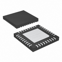
MAX8720ETX+ Maxim Integrated Products, MAX8720ETX+ Datasheet - Page 17

MAX8720ETX+
Manufacturer Part Number
MAX8720ETX+
Description
IC CNTRL VID STP DWN 36-TQFN
Manufacturer
Maxim Integrated Products
Datasheet
1.MAX8720ETXT.pdf
(31 pages)
Specifications of MAX8720ETX+
Applications
Controller, CPU GPU
Voltage - Input
2 ~ 28 V
Number Of Outputs
1
Voltage - Output
0.28 ~ 1.85 V
Operating Temperature
0°C ~ 85°C
Mounting Type
Surface Mount
Package / Case
36-TQFN Exposed Pad
Output Voltage
0.275 V to 1.85 V
Input Voltage
2 V to 28 V
Mounting Style
SMD/SMT
Maximum Operating Temperature
+ 85 C
Minimum Operating Temperature
- 40 C
Lead Free Status / RoHS Status
Lead free / RoHS Compliant
Figure 3. Pulse-Skipping/Discontinuous Crossover Point
Lot-to-lot variation of the threshold voltage can cause
problems in marginal designs. Typically, adding
4700pF between DL and power ground (C
5), close to the low-side MOSFETs, greatly reduces
coupling. Do not exceed 22nF of total gate capacitance
to prevent excessive turn-off delays.
Alternatively, shoot-through currents may be caused by
a combination of fast high-side MOSFETs and slow low-
side MOSFETs. If the turn-off delay time of the low-side
MOSFET is too long, the high-side MOSFETs can turn
on before the low-side MOSFETs have actually turned
off. Adding a resistor less than 5Ω in series with BST
slows down the high-side MOSFETs’ turn-on time, elimi-
nating the shoot-through currents without degrading
the turn-off time (R
high-side MOSFETs also reduces the LX node rise
time, thereby reducing EMI and high-frequency cou-
pling responsible for switching noise.
Power-on reset (POR) occurs when V
approximately 2V, resetting the fault latch and prepar-
ing the PWM for operation. V
(UVLO) circuitry inhibits switching, forces PGOOD low,
and forces the DL gate driver low. When V
above 4.2V, the DAC inputs are sampled and the out-
put voltage begins to slew to the DAC setting.
If V
is assumed that there is not enough supply voltage to
make valid decisions. The MAX8720 immediately forces
both DH and DL low. The output discharges to 0V at a
CC
drops low enough to trip the UVLO comparator, it
0
∆I
∆t
ON-TIME
=
V
V
GS TH
IN
______________________________________________________________________________________
- V
BST
L
(
OUT
)
in Figure 5). Slowing down the
>
V
TIME
IN
V
CC
C
C
RSS
CC
ISS
undervoltage-lockout
Dynamically Adjustable 6-Bit VID
POR and UVLO
I
I
CC
PEAK
LOAD
= I
NL
rises above
PEAK
in Figure
CC
/ 2
rises
rate dependent on the load and the total output capaci-
tance. This prevents negative output voltages, eliminat-
ing the need for a Schottky diode to GND at the output.
For automatic startup, the battery voltage should be
present before V
the output into regulation without the battery voltage
present, the fault latch trips. The SHDN pin can be tog-
gled to reset the fault latch.
Figure 4. Valley Current-Limit Threshold
Figure 5. Reducing the Switching-Node Rise Time
Step-Down Controller
(R
THE SWITCHING-NODE RISE TIME.
(C
COUPLING THAT CAN CAUSE SHOOT-THROUGH CURRENTS.
MAX8720
BST
NL
)* OPTIONAL—THE CAPACITOR REDUCES LX TO DL CAPACITIVE
)* OPTIONAL—THE RESISTOR LOWERS EMI BY DECREASING
V
DD
0
PGND
V
BST
DH
DL
DD
LX
CC
. If the MAX8720 attempts to bring
(R
BST
(C
I
C
LIM(VAL)
NL
BST
)*
)*
TIME
= I
LOAD(MAX)
D
C
BST
BYP
( )
N
N
1-
H
L
LIR
2
INPUT (V
L
I
I
I
PEAK
LOAD
LIMIT
IN
)
17


