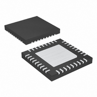
MAX8720ETX+ Maxim Integrated Products, MAX8720ETX+ Datasheet - Page 16

MAX8720ETX+
Manufacturer Part Number
MAX8720ETX+
Description
IC CNTRL VID STP DWN 36-TQFN
Manufacturer
Maxim Integrated Products
Datasheet
1.MAX8720ETXT.pdf
(31 pages)
Specifications of MAX8720ETX+
Applications
Controller, CPU GPU
Voltage - Input
2 ~ 28 V
Number Of Outputs
1
Voltage - Output
0.28 ~ 1.85 V
Operating Temperature
0°C ~ 85°C
Mounting Type
Surface Mount
Package / Case
36-TQFN Exposed Pad
Output Voltage
0.275 V to 1.85 V
Input Voltage
2 V to 28 V
Mounting Style
SMD/SMT
Maximum Operating Temperature
+ 85 C
Minimum Operating Temperature
- 40 C
Lead Free Status / RoHS Status
Lead free / RoHS Compliant
threshold between pulse-skipping PFM and nonskip-
ping PWM operation to coincide with the boundary
between continuous and discontinuous inductor-cur-
rent operation. The load-current level at which
PFM/PWM crossover occurs, I
half the peak-to-peak ripple current, which is a function
of the inductor value (Figure 3). For a 7V to 24V battery
range, this threshold is relatively constant, with only a
minor dependence on battery voltage:
where K is the on-time scale factor (Table 2). For exam-
ple, in the standard application circuit this becomes:
The crossover point occurs at a lower value if a swing-
ing (soft-saturation) inductor is used.
The switching waveforms may appear noisy and asyn-
chronous when light loading causes pulse-skipping
operation, but this is a normal operating condition that
results in high light-load efficiency. Trade-offs in PFM
noise vs. light-load efficiency are made by varying the
inductor value. Generally, low inductor values produce
a broader efficiency vs. load curve, while higher values
result in higher full-load efficiency (assuming that the
coil resistance remains fixed) and less output voltage
ripple. Penalties for using higher inductor values
include larger physical size and degraded load-tran-
sient response, especially at low input-voltage levels.
The current-limit circuit employs a unique “valley” cur-
rent-sensing algorithm that uses the on-resistance of
the low-side MOSFET as a current-sensing element. If
the current-sense signal is above the current-limit
threshold, the PWM is not allowed to initiate a new
cycle (Figure 4). The actual peak current is greater than
the current-limit threshold by an amount equal to the
inductor ripple current. Therefore, the exact current-
limit characteristic and maximum load capability are a
function of the MOSFET on-resistance, inductor value,
and battery voltage. The reward for this uncertainty is
robust, lossless overcurrent sensing. When combined
with the undervoltage-protection circuit, this current-
limit method is effective in almost every circumstance.
There is also a negative current limit that prevents
excessive reverse inductor currents when V
Dynamically Adjustable 6-Bit VID
Step-Down Controller
16
I
LOAD SKIP
______________________________________________________________________________________
(
I
LOAD SKIP
)
=
(
3 3
.
µ
)
s
2 0 8
=
×
×
1 25 12
KV
.
.
OUT IN
Current-Limit Circuit
V
µ
(
H
LOAD(SKIP)
2
(
×
V
LV
V
12
IN
−
−
V
1 25
V
.
OUT
V
, is equal to
)
)
=
2 31
.
OUT
A
is
sinking current. The negative current-limit threshold
is set to approximately 120% of the positive current
limit, and therefore tracks the positive current limit
when ILIM is adjusted.
The current-limit threshold is adjusted with an external
resistor-divider at ILIM. The current-limit threshold volt-
age adjustment range is from 50mV to 200mV. In the
adjustable mode, the current-limit threshold voltage is
precisely 1/10th the voltage seen at ILIM. The threshold
defaults to 100mV when ILIM is connected to V
logic threshold for switchover to the 100mV default
value is approximately V
Carefully observe the PC board layout guidelines to
ensure that noise and DC errors do not corrupt the cur-
rent-sense signals seen by LX and PGND. Place the IC
close to the low-side MOSFET with short, direct traces,
making a Kelvin-sense connection to the source and
drain terminals.
The DH and DL drivers are optimized for driving moder-
ate-sized high-side and larger low-side power MOSFETs.
This is consistent with the low duty factor seen in the
notebook CPU environment, where a large V
differential exists. An adaptive dead-time circuit monitors
the DL output and prevents the high-side FET from turn-
ing on until DL is fully off. There must be a low-resis-
tance, low-inductance path from the DL driver to the
MOSFET gate for the adaptive dead-time circuit to work
properly. Otherwise, the sense circuitry in the MAX8720
interprets the MOSFET gate as “off” while there is actual-
ly still charge left on the gate. Use very short, wide traces
measuring 10 to 20 squares (50 to 100 mils wide if the
MOSFET is 1in from the MAX8720).
The dead time at the other edge (DH turning off) is
determined by a fixed 35ns (typ) internal delay.
The internal pulldown transistor that drives DL low is
robust, with a 0.4Ω (typ) on-resistance. This helps pre-
vent DL from being pulled up during the fast rise time of
the inductor node, due to capacitive coupling from the
drain to the gate of the low-side synchronous-rectifier
MOSFET. Applications with high input voltages and
long, inductive DL traces may require additional gate-to-
source capacitance to ensure fast-rising LX edges do
not pull up the low-side MOSFET’s gate voltage, caus-
ing shoot-through currents. The capacitive coupling
between LX and DL created by the MOSFET’s gate-to-
drain capacitance (C
(C
not exceed the minimum threshold voltage:
ISS
- C
RSS
), and additional board parasitics should
MOSFET Gate Drivers (DH, DL)
RSS
CC
), gate-to-source capacitance
- 1V.
IN
CC
- V
. The
OUT


