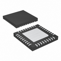
MAX8720ETX+ Maxim Integrated Products, MAX8720ETX+ Datasheet - Page 26

MAX8720ETX+
Manufacturer Part Number
MAX8720ETX+
Description
IC CNTRL VID STP DWN 36-TQFN
Manufacturer
Maxim Integrated Products
Datasheet
1.MAX8720ETXT.pdf
(31 pages)
Specifications of MAX8720ETX+
Applications
Controller, CPU GPU
Voltage - Input
2 ~ 28 V
Number Of Outputs
1
Voltage - Output
0.28 ~ 1.85 V
Operating Temperature
0°C ~ 85°C
Mounting Type
Surface Mount
Package / Case
36-TQFN Exposed Pad
Output Voltage
0.275 V to 1.85 V
Input Voltage
2 V to 28 V
Mounting Style
SMD/SMT
Maximum Operating Temperature
+ 85 C
Minimum Operating Temperature
- 40 C
Lead Free Status / RoHS Status
Lead free / RoHS Compliant
significantly higher, consider increasing the size of N
Conversely, if the losses at V
higher, consider reducing the size of N
not vary over a wide range, maximum efficiency is
achieved by selecting a high-side MOSFET (N
has conduction losses equal to the switching losses.
Choose a low-side MOSFET (N
possible on-resistance (R
ate-sized package (i.e., SO-8, DPAK, or D
reasonably priced. Ensure that the MAX8720 DL gate
driver can supply sufficient current to support the gate
charge and the current injected into the parasitic drain-
to-gate capacitor caused by the high-side MOSFET
turning on; otherwise, cross-conduction problems may
occur. Switching losses are not an issue for the low-
side MOSFET since it is a zero-voltage switched device
when used in the step-down topology.
Worst-case conduction losses occur at the duty-factor
extremes. For the high-side MOSFET (N
case power dissipation due to resistance occurs at the
minimum input voltage:
Generally, use a small high-side MOSFET to reduce
switching losses at high input voltages. However, the
R
pation limits often limits how small the MOSFET can be.
The optimum occurs when the switching losses equal
the conduction (R
losses do not become an issue until the input is greater
than approximately 15V.
Calculating the power dissipation in high-side
MOSFETs (N
it must allow for difficult-to-quantify factors that influ-
ence the turn-on and turn-off times. These factors
include the internal gate resistance, gate charge,
threshold voltage, source inductance, and PC board
layout characteristics. The following switching loss cal-
culation provides only a very rough estimate and is no
substitute for breadboard evaluation, preferably includ-
ing verification using a thermocouple mounted on N
where C
and I
(2A typ).
Dynamically Adjustable 6-Bit VID
Step-Down Controller
26
DS(ON)
PD N SWITCHING
PD N RESISTIVE
______________________________________________________________________________________
GATE
(
(
H
RSS
H
required to stay within package power-dissi-
is the peak gate-drive source/sink current
H
is the reverse transfer capacitance of N
) due to switching losses is difficult, since
DS(ON)
)
)
=
=
(
) losses. High-side switching
Power MOSFET Dissipation
V
V
DS(ON)
OUT
V
IN MAX
IN
(
IN(MAX)
L
(
), comes in a moder-
I
) that has the lowest
)
LOAD
)
2
I
GATE
C
RSS SW LOAD
are significantly
)
2
H
H
×
2
. If V
), the worst-
PAK), and is
f
R
DS ON
I
IN
(
H
) that
does
)
H
:
H
H
.
,
Switching losses in the high-side MOSFET can become
a heat problem when maximum AC-adapter voltages
are applied, due to the squared term in the switching-
loss equation (C x V
chosen for adequate R
becomes extraordinarily hot when subjected to
V
lower parasitic capacitance.
For the low-side MOSFET (N
dissipation always occurs at maximum battery voltage:
The absolute worst case for MOSFET power dissipation
occurs under heavy overload conditions that are
greater than I
exceed the current limit and cause the fault latch to trip.
To protect against this possibility, “overdesign” the cir-
cuit to tolerate:
where I
limit circuit, including threshold tolerance and sense-
resistance variation. The MOSFETs must have a
relatively large heatsink to handle the overload power
dissipation.
Choose a Schottky diode (D
drop low enough to prevent the low-side MOSFET’s
body diode from turning on during the dead time. As a
general rule, select a diode with a DC current rating
equal to 1/3rd of the load current. This diode is optional
and can be removed if efficiency is not critical.
The boost capacitors (C
enough to handle the gate-charging requirements of
the high-side MOSFETs. Typically, 0.1µF ceramic
capacitors work well for low-power applications driving
medium-sized MOSFETs. However, high-current appli-
cations driving large, high-side MOSFETs require boost
capacitors larger than 0.1µF. For these applications,
select the boost capacitors to avoid discharging the
capacitor more than 200mV while charging the high-
side MOSFETs’ gates:
PD N RESISTIVE
IN(MAX)
(
L
LIMIT
, consider choosing another MOSFET with
I
LOAD
is the peak current allowed by the current-
LOAD(MAX)
=
C
)
I
=
BST
LIMIT
IN
2 x f
1
−
DS(ON)
=
−
BST
N Q
SW
V
but are not high enough to
IN MAX
×
200
V
I
LOAD MAX
OUT
). If the high-side MOSFET
(
) must be selected large
L
L
) with a forward-voltage
), the worst-case power
GATE
mV
at low battery voltages
Boost Capacitors
)
(
2
(
I
LOAD
)
LIR
)
2
R
DS ON
(
)


