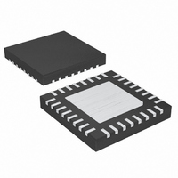
MAX8744ETJ+ Maxim Integrated Products, MAX8744ETJ+ Datasheet - Page 34

MAX8744ETJ+
Manufacturer Part Number
MAX8744ETJ+
Description
IC CNTRLR PWR SUP QUAD 32TQFN
Manufacturer
Maxim Integrated Products
Datasheet
1.MAX8745ETJT.pdf
(36 pages)
Specifications of MAX8744ETJ+
Applications
Controller, Notebook Computers
Voltage - Input
6 ~ 26 V
Number Of Outputs
4
Voltage - Output
3.3V, 5V, 1 ~ 26 V
Operating Temperature
0°C ~ 85°C
Mounting Type
Surface Mount
Package / Case
32-TQFN Exposed Pad
Duty Cycle (max)
99 %
Output Voltage
3.315 V, 5.015 V, 2 V to 5.5 V
Mounting Style
SMD/SMT
Switching Frequency
200 KHz, 300 KHz, 500 KHz
Maximum Operating Temperature
+ 85 C
Minimum Operating Temperature
- 40 C
Synchronous Pin
No
Topology
Boost, Flyback, Forward
Lead Free Status / RoHS Status
Lead free / RoHS Compliant
Careful PCB layout is critical to achieving low switching
losses and clean, stable operation. The switching
power stage requires particular attention (Figure 9). If
possible, mount all the power components on the top
side of the board, with their ground terminals flush
against one another. Follow these guidelines for good
PCB layout:
Keep the high-current paths short, especially at the
ground terminals. This practice is essential for stable,
jitter-free operation.
Keep the power traces and load connections short. This
practice is essential for high efficiency. Using thick cop-
per PCBs (2oz vs. 1oz) can enhance full-load efficiency
by 1% or more. Correctly routing PCB traces is a difficult
task that must be approached in terms of fractions of
centimeters, where a single milliohm of excess trace
resistance causes a measurable efficiency penalty.
Minimize current-sensing errors by connecting CSH_
and CSL_ directly across the current-sense resistor
(R
When trade-offs in trace lengths must be made, it is
preferable to allow the inductor charging path to be
made longer than the discharge path. For example, it is
better to allow some extra distance between the input
capacitors and the high-side MOSFET than to allow dis-
tance between the inductor and the low-side MOSFET
or between the inductor and the output filter capacitor.
Route high-speed switching nodes (BST_, LX_, DH_,
and DL_) away from sensitive analog areas (REF, FB_,
CSH_, CSL_).
High-Efficiency, Quad-Output, Main Power-
Supply Controllers for Notebook Computers
34
SENSE_
______________________________________________________________________________________
).
PCB Layout Guidelines
Place the power components first, with ground termi-
nals adjacent (N
anode). If possible, make all these connections on the
top layer with wide, copper-filled areas.
Mount the controller IC adjacent to the low-side MOSFET,
preferably on the back side opposite N
order to keep LX_, GND, DH_, and the DL_ gate-drive
lines short and wide. The DL_ and DH_ gate traces must
be short and wide (50 mils to 100 mils wide if the MOSFET
is 1in from the controller IC) to keep the driver impedance
low and for proper adaptive dead-time sensing.
Group the gate-drive components (BST_ diode and
capacitor, LDO5 bypass capacitor) together near the
controller IC.
Make the DC-DC controller ground connections as
shown in Figures 1 and 9. This diagram can be viewed
as having two separate ground planes: power ground,
where all the high-power components go, and an ana-
log ground plane for sensitive analog components. The
analog ground plane and power ground plane must
meet only at a single point directly at the IC.
Connect the output power planes directly to the output
filter capacitor positive and negative terminals with mul-
tiple vias. Place the entire DC-DC converter circuit as
close to the load as is practical.
L
_ source, C
Layout Procedure
IN
, C
OUT
L_
_, and D
and N
H_
L
in
_


