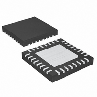
MAX8744ETJ+ Maxim Integrated Products, MAX8744ETJ+ Datasheet - Page 23

MAX8744ETJ+
Manufacturer Part Number
MAX8744ETJ+
Description
IC CNTRLR PWR SUP QUAD 32TQFN
Manufacturer
Maxim Integrated Products
Datasheet
1.MAX8745ETJT.pdf
(36 pages)
Specifications of MAX8744ETJ+
Applications
Controller, Notebook Computers
Voltage - Input
6 ~ 26 V
Number Of Outputs
4
Voltage - Output
3.3V, 5V, 1 ~ 26 V
Operating Temperature
0°C ~ 85°C
Mounting Type
Surface Mount
Package / Case
32-TQFN Exposed Pad
Duty Cycle (max)
99 %
Output Voltage
3.315 V, 5.015 V, 2 V to 5.5 V
Mounting Style
SMD/SMT
Switching Frequency
200 KHz, 300 KHz, 500 KHz
Maximum Operating Temperature
+ 85 C
Minimum Operating Temperature
- 40 C
Synchronous Pin
No
Topology
Boost, Flyback, Forward
Lead Free Status / RoHS Status
Lead free / RoHS Compliant
When adjusting both output voltages, set the 3.3V
SMPS lower than the 5V SMPS. LDO5 connects to the
5V output (CSL5) through an internal switch only when
CSL5 is above the LDO5 bootstrap threshold (4.5V)
and the soft-start sequence for the CSL5 side has com-
pleted. Bootstrapping works most effectively when the
fixed output voltages are used. Once LDO5 is boot-
strapped from CSL5, the internal 5V linear regulator
turns off. This reduces the internal power dissipation
and improves efficiency at higher input voltages.
The current-limit circuit uses differential current-sense
inputs (CSH_ and CSL_) to limit the peak inductor cur-
rent. If the magnitude of the current-sense signal
exceeds the current-limit threshold, the PWM controller
turns off the high-side MOSFET (Figure 3). The actual
maximum load current is less than the peak current-
limit threshold by an amount equal to half of the induc-
tor ripple current. Therefore, the maximum load
capability is a function of the current-sense resistance,
inductor value, switching frequency, and duty cycle
(V
In forced-PWM mode, the MAX8744/MAX8745 also
implement a negative current limit to prevent excessive
reverse inductor currents when V
The negative current-limit threshold is set to approxi-
mately 120% of the positive current limit and tracks the
positive current limit when ILIM is adjusted.
Connect ILIM to LDO5 for the 50mV default threshold,
or adjust the current-limit threshold with an external
resistor-divider at ILIM. Use a 2µA to 20µA divider cur-
rent for accuracy and noise immunity. The current-limit
threshold adjustment range is from 50mV to 200mV. In
the adjustable mode, the current-limit threshold voltage
equals precisely 1/10 the voltage seen at ILIM. The
logic threshold for switchover to the default value is
approximately V
Carefully observe the PCB layout guidelines to ensure
that noise and DC errors do not corrupt the differential
current-sense signals seen by CSH_ and CSL_. Place
the IC close to the sense resistor with short, direct
traces, making a Kelvin-sense connection to the cur-
rent-sense resistor.
OUT
/V
IN
).
Supply Controllers for Notebook Computers
High-Efficiency, Quad-Output, Main Power-
Current-Limit Protection (ILIM)
LDO5
______________________________________________________________________________________
- 1V.
OUT
is sinking current.
The DH_ and DL_ drivers are optimized for driving
moderate-sized high-side and larger low-side power
MOSFETs. This is consistent with the low duty factor
seen in notebook applications, where a large V
V
(DH_) source and sink 2A, and the low-side gate dri-
vers (DL_) source 1.7A and sink 3.3A. This ensures
robust gate drive for high-current applications. The
DH_ floating high-side MOSFET drivers are powered by
charge pumps at BST_ while the DL_ synchronous-rec-
tifier drivers are powered directly by the fixed 5V linear
regulator (LDO5).
Adaptive dead-time circuits monitor the DL_ and DH_
drivers and prevent either FET from turning on until the
other is fully off. The adaptive driver dead-time allows
operation without shoot-through with a wide range of
MOSFETs, minimizing delays and maintaining efficiency.
There must be a low-resistance, low-inductance path
from the DL_ and DH_ drivers to the MOSFET gates for
the adaptive dead-time circuits to work properly; other-
wise, the sense circuitry in the MAX8744/ MAX8745 inter-
prets the MOSFET gates as “off” while charge actually
remains. Use very short, wide traces (50 mils to 100 mils
wide if the MOSFET is 1in from the driver).
The internal pulldown transistor that drives DL_ low is
robust, with a 0.6Ω (typ) on-resistance. This helps prevent
DL_ from being pulled up due to capacitive coupling from
the drain to the gate of the low-side MOSFETs when the
Figure 6. Power-Good and Fault Protection
OUT
POWER-GOOD
0.9 x INT REF_
differential exists. The high-side gate drivers
MOSFET Gate Drivers (DH_, DL_)
6144
POR
CLK
0.7 x INT REF_
PROTECTION
FAULT
1.11 x INT REF_
LATCH
FAULT
INTERNAL FB
ENABLE OVP
ENABLE UVP
FAULT
POWER-GOOD
IN
23
-


