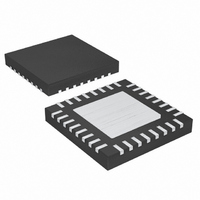
MAX8744ETJ+ Maxim Integrated Products, MAX8744ETJ+ Datasheet - Page 22

MAX8744ETJ+
Manufacturer Part Number
MAX8744ETJ+
Description
IC CNTRLR PWR SUP QUAD 32TQFN
Manufacturer
Maxim Integrated Products
Datasheet
1.MAX8745ETJT.pdf
(36 pages)
Specifications of MAX8744ETJ+
Applications
Controller, Notebook Computers
Voltage - Input
6 ~ 26 V
Number Of Outputs
4
Voltage - Output
3.3V, 5V, 1 ~ 26 V
Operating Temperature
0°C ~ 85°C
Mounting Type
Surface Mount
Package / Case
32-TQFN Exposed Pad
Duty Cycle (max)
99 %
Output Voltage
3.315 V, 5.015 V, 2 V to 5.5 V
Mounting Style
SMD/SMT
Switching Frequency
200 KHz, 300 KHz, 500 KHz
Maximum Operating Temperature
+ 85 C
Minimum Operating Temperature
- 40 C
Synchronous Pin
No
Topology
Boost, Flyback, Forward
Lead Free Status / RoHS Status
Lead free / RoHS Compliant
High-Efficiency, Quad-Output, Main Power-
Supply Controllers for Notebook Computers
a broader efficiency vs. load curve, while higher values
result in higher full-load efficiency (assuming that the
coil resistance remains fixed) and less output-voltage
ripple. Penalties for using higher inductor values
include larger physical size and degraded load-tran-
sient response (especially at low input-voltage levels).
DC output accuracy specifications in the Electrical
Characteristics table refer to the error comparator’s
threshold. When the inductor continuously conducts,
the MAX8744/MAX8745 regulate the peak of the output
ripple, so the actual DC output voltage is lower than the
slope-compensated trip level by 50% of the output rip-
ple voltage. For PWM operation (continuous conduc-
tion), the output voltage is accurately defined by the
following equation:
where V
equals 1%, and V
(V
Output Capacitor Selection section).
22
Figure 4. Pulse-Skipping/Discontinuous Crossover Point
V
RIPPLE
OUT PWM
______________________________________________________________________________________
0
(
NOM
= ESR x ΔI
ON-TIME
)
=
is the nominal output voltage, A
V
NOM
t
ON(SKIP)
RIPPLE
⎛
⎜
⎝
1
INDUCTOR
−
=
V
A
V
IN
OUT
f
SLOPE RIPPLE
is the output ripple voltage
OSC
TIME
V
IN
, as described in the
V
Output Voltage
⎞
⎟ −
⎠
⎛
⎜
⎝
I
I
V
PK
LOAD
RIPPLE
2
= I
SLOPE
PK
/2
⎞
⎟
⎠
In discontinuous conduction (I
MAX8744/MAX8745 regulate the valley of the output
ripple, so the output voltage has a DC regulation level
higher than the error-comparator threshold. For PFM
operation (discontinuous conduction), the output volt-
age is approximately defined by the following equation:
where V
maximum switching frequency set by the internal oscil-
lator, f
the idle mode inductor current when pulse skipping.
Connect FB3 and FB5 to LDO5 to enable the fixed
SMPS output voltages (3.3V and 5V, respectively), set
by a preset, internal resistive voltage-divider connected
between the output (CSL_) and analog ground.
Connect a resistive voltage-divider at FB_ between the
output (CSL_) and GND to adjust the respective output
voltage between 2V and 5.5V (Figure 5). Choose R
(resistance from FB to GND) to be approximately 10kΩ
and solve for R
using the equation:
where V
Figure 5. Dual Mode Feedback Decoder
SW
V
FB_
NOM
OUT PFM
LDO5
is the actual switching frequency, and I
OUT
FB
= 2V nominal.
AMPLIFIER
(
TO ERROR
is the nominal output voltage, f
R
FBHI
FBHI
9R
)
=
R
=
V
(resistance from the output to FB)
NOM
R
FBLO
+
FIXED OUTPUT
⎛
⎜
⎝
1
2
ADJUSTABLE
FB = LDO5
V
OUTPUT
⎛
⎜
⎝
V
OUT
OUT
f
FB
OSC
f
SW
_
_
< I
⎞
⎟
⎠
−
I
IDLE
1
⎞
⎟
⎠
LOAD(SKIP)
ESR
OSC
IDLE
is the
), the
FBLO
is


