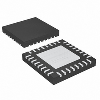
MAX8744ETJ+ Maxim Integrated Products, MAX8744ETJ+ Datasheet - Page 2

MAX8744ETJ+
Manufacturer Part Number
MAX8744ETJ+
Description
IC CNTRLR PWR SUP QUAD 32TQFN
Manufacturer
Maxim Integrated Products
Datasheet
1.MAX8745ETJT.pdf
(36 pages)
Specifications of MAX8744ETJ+
Applications
Controller, Notebook Computers
Voltage - Input
6 ~ 26 V
Number Of Outputs
4
Voltage - Output
3.3V, 5V, 1 ~ 26 V
Operating Temperature
0°C ~ 85°C
Mounting Type
Surface Mount
Package / Case
32-TQFN Exposed Pad
Duty Cycle (max)
99 %
Output Voltage
3.315 V, 5.015 V, 2 V to 5.5 V
Mounting Style
SMD/SMT
Switching Frequency
200 KHz, 300 KHz, 500 KHz
Maximum Operating Temperature
+ 85 C
Minimum Operating Temperature
- 40 C
Synchronous Pin
No
Topology
Boost, Flyback, Forward
Lead Free Status / RoHS Status
Lead free / RoHS Compliant
ABSOLUTE MAXIMUM RATINGS
High-Efficiency, Quad-Output, Main Power-
Supply Controllers for Notebook Computers
IN, SHDN, DRVA, OUTA to GND............................-0.3V to +28V
LDO5, ON3, ON5, ONA to GND ..............................-0.3V to +6V
PGOODA, PGOOD3, PGOOD5 to GND...................-0.3V to +6V
CSL3, CSH3, CSL5, CSH5 to GND ..........................-0.3V to +6V
REF, FB3, FB5, FBA to GND...................-0.3V to (V
SKIP, FSEL, ILIM to GND........................-0.3V to (V
DL3, DL5 to PGND..................................-0.3V to (V
BST3, BST5 to PGND .............................................-0.3V to +34V
BST3 to LX3..............................................................-0.3V to +6V
DH3 to LX3 ..............................................-0.3V to (V
BST5 to LX5..............................................................-0.3V to +6V
DH5 to LX5 ..............................................-0.3V to (V
GND to PGND .......................................................-0.3V to +0.3V
ELECTRICAL CHARACTERISTICS
(Circuit of Figure 1, V
no load, T
Stresses beyond those listed under “Absolute Maximum Ratings” may cause permanent damage to the device. These are stress ratings only, and functional
operation of the device at these or any other conditions beyond those indicated in the operational sections of the specifications is not implied. Exposure to
absolute maximum rating conditions for extended periods may affect device reliability.
2
INPUT SUPPLIES (Note 1)
V
V
V
V
Quiescent Power Consumption
MAIN SMPS CONTROLLERS
3.3V Output Voltage in Fixed
Mode
5V Output Voltage in Fixed Mode
Feedback Voltage in Adjustable
Mode (Note 2)
IN
IN
IN
IN
_______________________________________________________________________________________
Input Voltage Range
Operating Supply Current
Standby Supply Current
Shutdown Supply Current
A
PARAMETER
= 0°C to +85°C, unless otherwise noted. Typical values are at T
IN
= 12V, both SMPS enabled, FSEL = REF, SKIP = GND, ILIM = LDO5, FBA = LDO5, I
SYMBOL
I
I
IN(SHDN)
IN(STBY)
V
V
V
OUT3
OUT5
V
P
I
FB_
IN
IN
Q
LDO5
LDO5
LDO5
BST3
BST5
LDO5 in regulation
IN = LDO5, V
LDO5 switched over to CSL5, either
SMPS on
V
I
V
Both S M P S on, FB3 = FB5 = LD O5,
SKIP = GN D , V
V
P
V
0 < V
V
0 < V
V
duty factor = 20% to 80%
V
duty factor = 50%
SHDN
OU T A
IN
IN
IN
IN
IN
IN
IN
+ P
= 6V to 26V
= 6V to 26V, both SMPS off, includes
= 6V to 26V, SKIP = FB3 = LDO5,
= 6V to 26V, SKIP = FB5 = LDO5,
= 6V to 26V, FB3 or FB5
= 6V to 26V, FB3 or FB5
+ 0.3V)
+ 0.3V)
+ 0.3V)
+ 0.3V)
+ 0.3V)
CSH3
CSH5
= 15V ,
C S L 3
- V
- V
+ P
CSL5
CSL3
CSL5
CONDITIONS
C S L 3
C S L 5
BST3, BST5 LDO5 .................................................-0.3V to +0.3V
LDO Short Circuit to GND ..........................................Momentary
REF Short Circuit to GND ...........................................Momentary
DRVA Current (Sinking) ......................................................30mA
OUTA Shunt Current ...........................................................30mA
Continuous Power Dissipation (T
Multilayer PCB
Operating Temperature Range ...........................-40°C to +85°C
Junction Temperature ......................................................+150°C
Storage Temperature Range .............................-65°C to +150°C
Lead Temperature (soldering, 10s) ................................+300°C
< 4.4V
< 50mV (Note 2)
< 50mV (Note 2)
= 3.5V , V
+ P
32-Pin, 5mm x 5mm TQFN
(derated 34.5mW/°C above +70°C) .........................2459mW
A
OU T A
= +25°C.)
C S L 5
= 5.3V ,
3.265
1.980
1.990
4.94
MIN
5.4
4.5
A
= +70°C)
3.315
5.015
2.010
2.010
TYP
3.5
20
65
8
REF
= I
3.365
2.040
2.030
MAX
26.0
5.09
120
5.5
4.5
LDO5
36
20
= I
UNITS
OUTA
mW
µA
µA
µA
V
V
V
V
=


