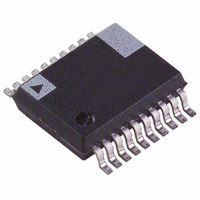
ADE7756ARS Analog Devices Inc, ADE7756ARS Datasheet - Page 29

ADE7756ARS
Manufacturer Part Number
ADE7756ARS
Description
IC ENERGY METERING 1PHASE 20SSOP
Manufacturer
Analog Devices Inc
Datasheet
1.ADE7756AN.pdf
(32 pages)
Specifications of ADE7756ARS
Rohs Status
RoHS non-compliant
Input Impedance
390 KOhm
Measurement Error
0.1%
Voltage - I/o High
2.4V
Voltage - I/o Low
0.8V
Current - Supply
3mA
Voltage - Supply
4.75 V ~ 5.25 V
Operating Temperature
-40°C ~ 85°C
Mounting Type
Surface Mount
Package / Case
20-SSOP (0.200", 5.30mm Width)
Meter Type
Single Phase
Lead Free Status / RoHS Status
Not Compliant
Available stocks
Company
Part Number
Manufacturer
Quantity
Price
Company:
Part Number:
ADE7756ARSZ
Manufacturer:
AD
Quantity:
17 677
Part Number:
ADE7756ARSZ
Manufacturer:
ADI/亚德诺
Quantity:
20 000
Address
10H
11H
12H
REGISTER DESCRIPTIONS
All ADE7756 functionality is accessed via the on-chip registers. Each register is accessed by first writing to the communications
register and then transferring the register data. A full description of the serial interface protocol is given in the Serial Interface section
of this data sheet.
Communications Register
The Communications register is an 8-bit, write-only register that controls the serial data transfer between the ADE7756 and the host
processor. All data transfer operations must begin with a write to the communications register. The data written to the communica-
tions register determines whether the next operation is a read or a write and which register is being accessed. Table V outlines the bit
designations for the Communications register.
Bit
Location
5 to 6
7
0 to 4
Name
IRQEN
SAGLVL
TEMP
DB7
W/R
Bit
Mnemonic
A0 to A4
RESERVED
W/R
DB6
0
R/W
R/W
R/W
R
Description
The five LSBs of the Communications register specify the register for the data transfer opera-
tion. Table IV lists the address of each ADE7756 on-chip register.
These bits are unused and should be set to zero.
When this bit is a Logic 1, the data transfer operation immediately following the write to the
Communications register will be interpreted as a write to the ADE7756. When this bit is a
Logic 0, the data transfer operation immediately following the write to the Communications
register will be interpreted as a read operation.
No. of
Bits
8
8
8
DB5
0
Table V. Communications Register
Table IV. Register List (continued)
Default
0h
0h
0h
DB4
A4
Description
Interrupt Enable Register. ADE7756 interrupts may be deactivated at
any time by setting the corresponding bit in this 8-bit Enable register
Logic 0. The Status register will continue to register an interrupt event
even if disabled. However, the IRQ output will not be activated
—see Interrupts section.
Sag Voltage Level. An 8-bit write to this register determines at what
peak signal level on Channel 2 the SAG pin will become active. The
signal must remain low for the number of cycles specified in the SAGCYC
register before the SAG pin is activated—see Line Voltage Sag Detec-
tion section.
Temperature Register. This is an 8-bit register which contains the result
of the latest temperature conversion. A full description of this register’s
contents can be found in the Temperature Measurement section of this
data sheet.
DB3
A3
DB2
A2
DB1
A1
DB0
A0
ADE7756


