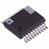
ADE7756ARS Analog Devices Inc, ADE7756ARS Datasheet - Page 18

ADE7756ARS
Manufacturer Part Number
ADE7756ARS
Description
IC ENERGY METERING 1PHASE 20SSOP
Manufacturer
Analog Devices Inc
Datasheet
1.ADE7756AN.pdf
(32 pages)
Specifications of ADE7756ARS
Rohs Status
RoHS non-compliant
Input Impedance
390 KOhm
Measurement Error
0.1%
Voltage - I/o High
2.4V
Voltage - I/o Low
0.8V
Current - Supply
3mA
Voltage - Supply
4.75 V ~ 5.25 V
Operating Temperature
-40°C ~ 85°C
Mounting Type
Surface Mount
Package / Case
20-SSOP (0.200", 5.30mm Width)
Meter Type
Single Phase
Lead Free Status / RoHS Status
Not Compliant
Available stocks
Company
Part Number
Manufacturer
Quantity
Price
Company:
Part Number:
ADE7756ARSZ
Manufacturer:
AD
Quantity:
17 677
Part Number:
ADE7756ARSZ
Manufacturer:
ADI/亚德诺
Quantity:
20 000
ADE7756
CHANNEL 1 ADC
Figure 18 shows the ADC and signal processing chain for Chan-
nel 1. In waveform sampling mode the ADC outputs a signed
two’s complement 20-bit data word at a maximum of 27.9 kSPS
(CLKIN/128). The output of the ADC can be scaled by ± 50% to
perform an overall power calibration or to calibrate the ADC out-
put. While the ADC outputs a 20-bit two’s complement value, the
maximum full-scale positive value from the ADC is limited to
40000h (+262,144 decimal). The maximum full-scale negative
value is limited to C0000h (–262,144 Decimal). If the analog
inputs are overranged, the ADC output code will clamp at these
values. With the specified full scale analog input signal of 1 V (or
0.5 V or 0.25 V—see Analog Inputs section) the ADC will produce
an output code which is approximately 63% of its full-scale value.
This is illustrated in Figure 18. The diagram in Figure 15 shows
a full-scale voltage signal being applied to the differential inputs
V1P and V1N. The ADC output swings between D7AE1h
(–165,151) and 2851Fh (+165,151). This is approximately 63%
of the full-scale value 40000h (262,144). Overranging the analog
inputs with more than 1 V differential (0.5 or 0.25, depending
on Channel 1 full-scale selection) will cause the ADC output to
increase towards its full-scale value. However for specified opera-
tion the differential signal on the analog inputs should not exceed
the recommended value of 1.0 V.
Channel 1 ADC Gain Adjust
The ADC gain in Channel 1 can be adjusted by using the multi-
plier and Active Power Gain register (APGAIN[11:0]). The
gain of the ADC is adjusted by writing a two’s complement
12-bit word to the Active Power Gain register. Following is
62.5mV, 31.3mV, 15.6mV
1V, 0.5V, 0.25V, 125mV,
V1
0V
V1N
V1P
ANALOG INPUT
RANGE
x1, x2, x4,
x8, x16
GAIN[2:0]
PGA1
2.42V, 1.21V, 0.6V
D7AE1h
C0000h
2851Fh
REFERENCE
40000h
00000h
ADC
ADC OUTPUT
WORD RANGE
801Hex – 7FFHex
MULTIPLIER
APGAIN[11:0]
1
GAIN[4:3]
the expression that shows how the gain adjustment is related to
the contents of the Active Power Gain register.
For example when 7FFh is written to the Active Power Gain
register the ADC output is scaled up by 50%. 7FFh = 2047 deci-
mal, 2047/2
two’s complement) and ADC output is scaled by –50%. These
two examples are graphically illustrated in Figure 18.
Channel 1 Sampling
The waveform samples may also be routed to the Waveform
register (MODE[14:13] = 1, 0) to be read by the system master
(MCU). In waveform sampling mode the WSMP bit (Bit 3) in
the Interrupt Enable register must also be set to Logic 1. The
Active Power and Energy calculation will remain uninterrupted
during waveform sampling.
When in waveform sample mode, one of four output sample rates
may be chosen by using Bits 11 and 12 of the Mode register
(WAVSEL1, 0). The output sample rate may be 27.9 kSPS,
14 kSPS, 7 kSPS or 3.5 kSPS—see Mode Register section. The
interrupt request output IRQ signals a new sample availability
by going active low. The timing is shown in Figure 19. The
20-bit waveform samples are transferred from the ADE7756 one
byte (8 bits) at a time, with the most significant byte shifted out
first. The 20-bit data word is right-justified and sign extended
to 24 bits (three bytes)—see Serial Interface section.
+FS
+63% FS
–63% FS
–FS
12
1
DIGITAL
SINC
LPF
3
12
3C7AEh
EBD71h
D7AE1h
C3852h
2851Fh
1428Fh
00000h
Code
= 0.5. Similarly, 801h = –2047 decimal (signed
20
HPF
=
000h 7FFh 801h
APGAIN[11:0]
CHANNEL 1 (ACTIVE POWER)
CALIBRATION RANGE
ADC
×
TO
MULTIPLIER
WAVEFORM[23:0]
TO
WAVEFORM
REGISTER
1
+94.5% FS
+63% FS
+31.5% FS
–31.5% FS
–63% FS
–94.5% FS
+
APGAIN
2
12


