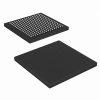
CYD09S18V18-167BBXI Cypress Semiconductor Corp, CYD09S18V18-167BBXI Datasheet - Page 49

CYD09S18V18-167BBXI
Manufacturer Part Number
CYD09S18V18-167BBXI
Description
IC SRAM 9MBIT 167MHZ 256LFBGA
Manufacturer
Cypress Semiconductor Corp
Datasheet
1.CYD02S36V18-167BBC.pdf
(52 pages)
Specifications of CYD09S18V18-167BBXI
Format - Memory
RAM
Memory Type
SRAM - Dual Port, Synchronous
Memory Size
9M (512K x 18)
Speed
167MHz
Interface
Parallel
Voltage - Supply
1.42 V ~ 1.58 V, 1.7 V ~ 1.9 V
Operating Temperature
-40°C ~ 85°C
Package / Case
256-LFBGA
Lead Free Status / RoHS Status
Lead free / RoHS Compliant
Available stocks
Company
Part Number
Manufacturer
Quantity
Price
Company:
Part Number:
CYD09S18V18-167BBXI
Manufacturer:
Cypress Semiconductor Corp
Quantity:
135
Company:
Part Number:
CYD09S18V18-167BBXI
Manufacturer:
Cypress Semiconductor Corp
Quantity:
10 000
Document History Page
Document Number: 38-06082 Rev. *J
Document Title: FullFlex™ Synchronous SDR Dual Port SRAM
Document Number: 38-06082
REV.
*A
*B
**
ECN NO. Submission
334036
395800
302411
See ECN
See ECN
See ECN
Date
Orig. of
Change
YDT
YDT
SPN
New data sheet
Corrected typo on page 1
Reproduced PDF file to fix formatting errors
Added statement about no echo clocks for flow through mode
Updated electrical characteristics
Added note 16 and 17 (1.5 V timing)
Added note 33 (timing for x18 devices)
Updated input edge rate (note 34)
Updated table 5 on deterministic access control logic
Added description of busy readback in deterministic access control section
Changed dummy write descriptions
Updated ZQ pins connection details
Updated note 24, B0 to BE0
Added power supply requirements to MRST and VC_SEL
Added note 4 (VIM disable)
Updated supply voltage to ground potential to 4.1 V
Updated parameters on table 15
Updated and added parameters to table 16
Updated x72 pinout to SDR only pinout
Updated 484 PBGA pin diagram
Updated the pin definition of MRST
Updated the pin definition of VC_SEL
Updated READY description to include Wired OR note
Updated master reset to include wired OR note for READY
Updated minimum V
Updated electrical characteristics to include I
Updated electrical characteristics to include READY
Added I
Updated maximum input capacitance
Added Notes 33 and 34Removed Notes 15 and 17
Updated Pin Definitions for CQ0, CQ0
Removed -100 Speed bin from Table.1 Selection Guide
Changed voltage name from V
Changed voltage name from V
Moved the Mailbox Interrupt Timing Diagram to be the final timing diagram
Updated the Package Type for the CYD36S18V18 parts
Updated the Package Type for the CYD36S18V18 parts
Updated the Package Type for the CYD18S18V18 parts
Updated the Package Type for the CYD18S36V18 parts
Included the Package Diagram for the 256-Ball FBGA (19 x 19 mm) BW256
Included an OE Controlled Write for Flow through Mode Switching Waveform
Included a Read with Echo Clock Switching Waveform
Updated Figure 5 and Figure 6
Updated Electrical Characteristics for READY V
Updated Electrical Characteristics for V
Included a Unit column for Table 5
Removed Switching Characteristic t
Included t
Included t
IX3
OHZ
CKLZ2
in Switching Waveform OE Controlled Write for Pipelined Mode
in Waveform Read-to-Write-to-Read for Flow through Mode
OH
value for the 1.8 V LVCMOS configuration
Description of Change
DDQ
DD
to V
to V
CA
CORE
,
from chart
CQ1
OH
DDIO
and V
,
OH
and CQ1
OH
and I
OL
and READY V
for the -167 and -133 speeds
OL
values
Page 49 of 52
FullFlex
[+] Feedback


