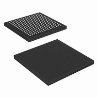
CYD09S18V18-167BBXI Cypress Semiconductor Corp, CYD09S18V18-167BBXI Datasheet - Page 18

CYD09S18V18-167BBXI
Manufacturer Part Number
CYD09S18V18-167BBXI
Description
IC SRAM 9MBIT 167MHZ 256LFBGA
Manufacturer
Cypress Semiconductor Corp
Datasheet
1.CYD02S36V18-167BBC.pdf
(52 pages)
Specifications of CYD09S18V18-167BBXI
Format - Memory
RAM
Memory Type
SRAM - Dual Port, Synchronous
Memory Size
9M (512K x 18)
Speed
167MHz
Interface
Parallel
Voltage - Supply
1.42 V ~ 1.58 V, 1.7 V ~ 1.9 V
Operating Temperature
-40°C ~ 85°C
Package / Case
256-LFBGA
Lead Free Status / RoHS Status
Lead free / RoHS Compliant
Available stocks
Company
Part Number
Manufacturer
Quantity
Price
Company:
Part Number:
CYD09S18V18-167BBXI
Manufacturer:
Cypress Semiconductor Corp
Quantity:
135
Company:
Part Number:
CYD09S18V18-167BBXI
Manufacturer:
Cypress Semiconductor Corp
Quantity:
10 000
Master Reset
The FullFlex family of Dual Ports undergoes a complete reset
when MRST is asserted. MRST must be driven by VDDIO
referenced levels. The MRST is asserted asynchronously to the
clocks and must remain asserted for at least t
MRST deasserts READY, initializes the internal burst counters,
internal mirror registers, and internal busy addresses to zero. It
also initializes the internal mask register to all 1s. All mailbox
interrupts (INT), busy address outputs (BUSY), and burst
counter interrupts (CNTINT) are deasserted upon master reset.
Additionally, do not release MRST until all power supplies
including VREF are fully ramped and all port clocks and mode
select inputs (LOWSPD, ZQ, CQEN, FTSEL, and PORTSTD)
are valid and stable. This begins calibration of the DLL and VIM
circuits. READY is asserted within 1024 clock cycles. READY is
a wired OR capable output with a strong pull up and weak pull
down. Up to four outputs may be connected together. For faster
pull down of the signal, connect a 250 Ohm resistor to VSS. If
the DLL and VIM circuits are disabled for a port, the port is
operational within five clock cycles. However, the READY is
asserted within 160 clock cycles.
IEEE 1149.1 Serial Boundary Scan (JTAG)
The FullFlex families incorporate an IEEE 1149.1 serial
boundary scan test access port (TAP). The TAP operates using
JEDEC-standard 3.3 V or 2.5 V IO logic levels depending on the
VTTL power supply. It is composed of four input connections and
one output connection required by the test logic defined by the
standard.
Table 11. Instruction Identification Codes
Note
Document Number: 38-06082 Rev. *J
EXTEST
BYPASS
IDCODE
HIGHZ
CLAMP
SAMPLE/PRELOAD
RESERVED
38. Details of the boundary scan length is found in the BSDL file for the device.
Instruction
All other
codes
Code
0000
0100
1000
1011
0111
1111
Captures the input and output ring contents. Places the BSR between the TDI and TDO.
Places the BYR between TDI and TDO.
Loads the IDR with the vendor ID code and places the register between TDI and TDO.
Places BYR between TDI and TDO. Forces all FullFlex72 and FullFlex36 output drivers to a
High Z state.
Controls boundary to 1 or 0. Places BYR between TDI and TDO.
Captures the input and output ring contents. Places BSR between TDI and TDO.
Other combinations are reserved. Do not use other than the mentioned combinations.
RS
. When asserted
L
Table 9. JTAG IDCODE Register Definitions
Table 10. Scan Registers Sizes
CYD36S72V18
CYD36S36V18
CYD36S18V18
CYD18S72V18
CYD18S36V18
CYD18S18V18
CYD09S72V18
CYD09S36V18
CYD09S18V18
CYD04S72V18
CYD04S36V18
CYD04S18V18
CYD02S36V18
Instruction
Bypass
Identification
Boundary Scan
Part Number
Register Name
Description
Configuration
1024 K × 36
2048 K × 36
1024 K × 18
512 K × 72
256 K × 72
512 K × 36
128 K × 72
256 K × 36
512 K × 18
128 K × 36
256 K × 18
64 K × 72
64 K × 36
Bit Size
n
32
0C026069h (x2)
[38]
0C02A069h
0C02B069h
0C02C069h
0C02D069h
0C023069h
0C024069h
0C025069h
0C026069h
0C027069h
0C028069h
0C029069h
0C030069h
4
1
Page 18 of 52
FullFlex
Value
[+] Feedback


