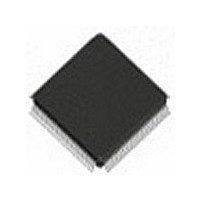
IDT72V845L15PFI IDT, Integrated Device Technology Inc, IDT72V845L15PFI Datasheet - Page 5

IDT72V845L15PFI
Manufacturer Part Number
IDT72V845L15PFI
Description
IC FIFO SYNC 4096X18 128QFP
Manufacturer
IDT, Integrated Device Technology Inc
Series
72Vr
Datasheet
1.IDT72V805L20PF8.pdf
(26 pages)
Specifications of IDT72V845L15PFI
Function
Asynchronous, Synchronous
Memory Size
72K (4K x 18)
Data Rate
67MHz
Access Time
15ns
Voltage - Supply
3 V ~ 3.6 V
Operating Temperature
-40°C ~ 85°C
Mounting Type
Surface Mount
Package / Case
128-TQFP, 128-VQFP
Configuration
Quad
Density
144Kb
Access Time (max)
10ns
Word Size
18b
Organization
4Kx18x2
Sync/async
Synchronous
Expandable
Yes
Bus Direction
Bi-Directional
Package Type
TQFP
Clock Freq (max)
66.7MHz
Operating Supply Voltage (typ)
3.3V
Operating Supply Voltage (min)
3V
Operating Supply Voltage (max)
3.6V
Supply Current
60mA
Operating Temp Range
-40C to 85C
Operating Temperature Classification
Industrial
Mounting
Surface Mount
Pin Count
128
Lead Free Status / RoHS Status
Contains lead / RoHS non-compliant
Other names
72V845L15PFI
Available stocks
Company
Part Number
Manufacturer
Quantity
Price
Company:
Part Number:
IDT72V845L15PFI
Manufacturer:
IDT
Quantity:
221
Company:
Part Number:
IDT72V845L15PFI
Manufacturer:
IDT, Integrated Device Technology Inc
Quantity:
10 000
Company:
Part Number:
IDT72V845L15PFI8
Manufacturer:
IDT, Integrated Device Technology Inc
Quantity:
10 000
AC ELECTRICAL CHARACTERISTICS
(Commercial: V
NOTES:
1. Pulse widths less than minimum values are not allowed.
2. Industrial temperature range product for the 15ns speed grade is available as a standard device.
3. Values guaranteed by design, not currently tested.
4. t
AC TEST CONDITIONS
IDT72V805/72V815/72V825/72V835/72V845
3.3 V CMOS DUAL SyncFIFO™ 256 x 18, 512 x 18, 1,024 x 18, 4,096 x 18
Symbol
f
t
t
t
t
t
t
t
t
t
t
t
t
t
t
t
t
t
t
t
t
t
t
t
t
t
t
t
Input Pulse Levels
Input Rise/Fall Times
Input Timing Reference Levels
Output Reference Levels
Output Load
S
A
CLK
CLKH
CLKL
DS
DH
ENS
ENH
RS
RSS
RSR
RSF
OLZ
OE
OHZ
WFF
REF
PAFA
PAFS
PAEA
PAES
HF
XO
XI
XIS
SKEW1
SKEW2
SKEW2
(4)
applies to synchronous PAE and synchronous PAF only.
Clock Cycle Frequency—
Data Access Time
Clock Cycle Time
Clock HIGH Time
Clock LOW Time
Data Setup Time
Data Hold Time
Enable Setup Time
Enable Hold Time
Reset Pulse Width
Reset Setup Time
Reset Recovery Time
Reset to Flag and Output Time
Output Enable to Output in Low-Z
Output Enable to Output Valid
Output Enable to Output in High-Z
Write Clock to Full Flag
Read Clock to Empty Flag
Clock to Asynchronous Programmable
Almost-Full Flag
Write Clock to Synchronous
Programmable Almost-Full Flag
Clock to Asynchronous Programmable
Almost-Empty Flag
Read Clock to Synchronous
Programmable Almost-Empty Flag
Clock to Half-Full Flag
Clock to Expansion Out
Expansion In Pulse Width
Expansion In Setup Time
Skew time between Read Clock &
Write Clock for FF/IR and EF/OR
Skew time between Read Clock &
Write Clock for PAE and PAF
CC
= 3.3V ± 0.3V, T
Parameter
(1)
A
= 0°C to +70°C; Industrial: V
(3)
(3)
GND to 3.0V
See Figure 1
1.5V
1.5V
3ns
Min.
100
4.5
4.5
0.5
0.5
10
10
—
—
—
—
—
—
—
—
—
—
14
IDT72V805L10
IDT72V815L10
IDT72V825L10
IDT72V835L10
IDT72V845L10
2
3
3
8
8
0
1
3
3
5
Commercial
CC
= 3.3V ± 0.3V, TA = -40°C to +85°C)
5
Max.
6.5
6.5
6.5
6.5
15
17
17
17
—
—
—
—
—
—
—
—
—
—
—
—
—
—
—
—
6
6
8
8
D.U.T.
Min.
66.7
6.5
Com’l & Ind’l
15
15
10
10
18
—
—
—
—
—
—
—
—
—
2
6
6
4
1
4
1
0
3
3
5
6
IDT72V815L15
IDT72V825L15
IDT72V835L15
IDT72V845L15
IDT72V805L15
* Includes jig and scope capacitances.
510Ω
Figure 1. Output Load
Max.
10
15
10
10
20
10
20
10
20
10
—
—
—
—
—
—
—
—
—
—
—
—
—
—
—
—
8
8
(2)
COMMERCIAL AND INDUSTRIAL
Min.
50
20
20
12
12
20
3.3V
IDT72V815L20
IDT72V825L20
IDT72V835L20
IDT72V845L20
—
—
—
—
—
—
—
—
—
IDT72V805L20
2
8
8
5
1
5
1
0
3
3
8
8
8
Commercial
TEMPERATURE RANGES
330Ω
30pF*
FEBRUARY 11, 2009
4295 drw 03
Max.
MHz
12
—
20
10
10
12
12
22
12
22
12
22
12
—
—
—
—
—
—
—
—
—
—
—
—
—
—
Unit
ns
ns
ns
ns
ns
ns
ns
ns
ns
ns
ns
ns
ns
ns
ns
ns
ns
ns
ns
ns
ns
ns
ns
ns
ns
ns
ns


