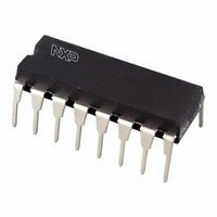
74HC40105N,652 NXP Semiconductors, 74HC40105N,652 Datasheet - Page 5

74HC40105N,652
Manufacturer Part Number
74HC40105N,652
Description
IC FIFO REGISTER 4X16 16DIP
Manufacturer
NXP Semiconductors
Series
74HCr
Datasheet
1.74HC40105DB118.pdf
(25 pages)
Specifications of 74HC40105N,652
Function
Asynchronous
Memory Size
64 (4 x 16)
Data Rate
25MHz
Voltage - Supply
2 V ~ 6 V
Mounting Type
Through Hole
Package / Case
16-DIP (0.300", 7.62mm)
Logic Family
HC
Logical Function
FIFO Register
Number Of Elements
1
Number Of Bits
4
Number Of Inputs
4
Number Of Outputs
4
High Level Output Current
-7.8mA
Low Level Output Current
7.8mA
Propagation Delay Time
750ns
Operating Supply Voltage (typ)
5V
Operating Supply Voltage (max)
6V
Operating Supply Voltage (min)
2V
Output Type
3-State
Polarity
Non-Inverting
Technology
CMOS
Frequency (max)
36(Typ)MHz
Mounting
Through Hole
Pin Count
16
Operating Temp Range
-40C to 125C
Operating Temperature Classification
Automotive
Quiescent Current
8uA
Lead Free Status / RoHS Status
Lead free / RoHS Compliant
Operating Temperature
-
Access Time
-
Lead Free Status / Rohs Status
Compliant
Other names
74HC40105N
74HC40105N
933669660652
74HC40105N
933669660652
Philips Semiconductors
data moves through the FIFO to the
output stage, resulting in the DOR
flag pulsing HIGH and a shift-out of
data occurring. The SO control must
be made LOW before additional data
can be shifted-out (see Fig.10).
High-speed burst mode
If it is assumed that the
shift-in/shift-out pulses are not
applied until the respective status
flags are valid, it follows that the
shift-in/shift-out rates are determined
by the status flags. However, without
the status flags a high-speed burst
mode can be implemented. In this
mode, the burst-in/ burst-out rates are
determined by the pulse widths of the
shift-in/shift-out inputs and burst rates
of 35 MHz can be obtained. Shift
1998 Jan 23
4-bit x 16-word FIFO register
pulses can be applied without regard
to the status flags but shift-in pulses
that would overflow the storage
capacity of the FIFO are not allowed
(see Figs 11 and 12).
Expanded format
With the addition of a logic gate, the
FIFO is easily expanded to increase
word length (see Fig.17). The basic
operation and timing are identical to a
single FIFO, with the exception of an
additional gate delay on the flag
outputs. If during application, the
following occurs:
SI is held HIGH when the FIFO is
empty, some additional logic is
required to produce a composite
DIR pulse (see Figs 7 and 18).
5
Due to the part-to-part spread of the
ripple through time, the SI signals of
FIFO
coincide and the AND-gate will not
produce a composite flag signal. The
solution is given in Fig.18.
The “40105” is easily cascaded to
increase the word capacity and no
external components are needed. In
the cascaded configuration, all
necessary communications and
timing are performed by the FIFOs.
The intercommunication speed is
determined by the minimum flag
pulse widths and the flag delays. The
data rate of cascaded devices is
typically 25 MHz. Word-capacity can
be expanded to and beyond 32-words
4-bits (see Fig.19).
A
and FIFO
74HC/HCT40105
Product specification
B
will not always


