74HC40105N,652 NXP Semiconductors, 74HC40105N,652 Datasheet - Page 4
74HC40105N,652
Manufacturer Part Number
74HC40105N,652
Description
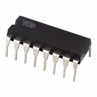
IC FIFO REGISTER 4X16 16DIP
Manufacturer
NXP Semiconductors
Series
74HCr
Datasheet
1.74HC40105DB118.pdf
(25 pages)
Specifications of 74HC40105N,652
Function
Asynchronous
Memory Size
64 (4 x 16)
Data Rate
25MHz
Voltage - Supply
2 V ~ 6 V
Mounting Type
Through Hole
Package / Case
16-DIP (0.300", 7.62mm)
Logic Family
HC
Logical Function
FIFO Register
Number Of Elements
1
Number Of Bits
4
Number Of Inputs
4
Number Of Outputs
4
High Level Output Current
-7.8mA
Low Level Output Current
7.8mA
Propagation Delay Time
750ns
Operating Supply Voltage (typ)
5V
Operating Supply Voltage (max)
6V
Operating Supply Voltage (min)
2V
Output Type
3-State
Polarity
Non-Inverting
Technology
CMOS
Frequency (max)
36(Typ)MHz
Mounting
Through Hole
Pin Count
16
Operating Temp Range
-40C to 125C
Operating Temperature Classification
Automotive
Quiescent Current
8uA
Lead Free Status / RoHS Status
Lead free / RoHS Compliant
Operating Temperature
-
Access Time
-
Lead Free Status / Rohs Status
Compliant
Other names
74HC40105N
74HC40105N
933669660652
74HC40105N
933669660652


Philips Semiconductors
INPUT AND OUTPUTS
Data inputs (D
As there is no weighting of the inputs,
any input can be assigned as the
MSB. The size of the FIFO memory
can be reduced from the 4
configuration, i.e. 3
1
pins to V
Data outputs (Q
As there is no weighting of the
outputs, any output can be assigned
as the MSB. The size of the FIFO
memory can be reduced from the
4
data inputs. In a reduced format, the
unused data outputs pins must be left
open circuit.
Master-reset (MR)
When MR is HIGH, the control
functions within the FIFO are cleared,
and date content is declared invalid.
The data-in ready (DIR) flag is set
HIGH and the data-out-ready (DOR)
flag is set LOW. The output stage
remains in the state of the last word
that was shifted out, or in the random
state existing at power-up.
Status flag outputs (DIR, DOR)
Indication of the status of the FIFO is
given by two status flags,
data-in-ready (DIR) and
data-out-ready (DOR):
DIR = HIGH indicates the input stage
is empty and ready to accept valid
data;
DIR = LOW indicates that the FIFO is
full or that a previous shift-in
operation is not complete (busy);
DOR = HIGH assures valid data is
present at the outputs Q
not indicate that new data is awaiting
transfer into the output stage);
DOR = LOW indicates the output
stage is busy or there is no valid data.
1998 Jan 23
4-bit x 16-word FIFO register
16, by tying unused data input
16 configuration as described for
CC
or GND.
0
to D
0
to Q
3
16, down to
)
3
0
)
to Q
16
3
(does
Shift-in control (SI)
Data is loaded into the input stage on
a LOW-to-HIGH transition of SI.
It also triggers an automatic data
transfer process (ripple through). If SI
is held HIGH during reset, data will be
loaded at the falling edge of the MR
signal.
Shift-out control (SO)
A HIGH-to-LOW transition of
SO causes the DOR flags to go LOW.
A HIGH-to-LOW transition of
SO causes upstream data to move
into the output stage, and empty
locations to move towards the input
stage (bubble-up).
Output enable (OE)
The outputs Q
when OE = LOW. When OE = HIGH
the outputs are in the high impedance
OFF-state.
FUNCTIONAL DESCRIPTION
Data input
Following power-up, the master-reset
(MR) input is pulsed HIGH to clear the
FIFO memory (see Fig.8). The
data-in-ready flag (DIR = HIGH)
indicates that the FIFO input stage is
empty and ready to receive data.
When DIR is valid (HIGH), data
present at D
using the SI control input.
With SI = HIGH, data is shifted into
the input stage and a busy indication
is given by DIR going LOW.
The data remains at the first location
in the FIFO until DIR is set to HIGH
and data moves through the FIFO to
the output stage, or to the last empty
location. If the FIFO is not full after the
SI pulse, DIR again becomes valid
(HIGH) to indicate that space is
available in the FIFO. The DIR flag
remains LOW if the FIFO is full (see
Fig.6). The SI use must be made
0
to D
0
to Q
3
4
can be shifted-in
3
are enabled
LOW in order to complete the shift-in
process.
With the FIFO full, SI can be held
HIGH until a shift-out (SO) pulse
occurs. Then, following a shift-out of
data, an empty location appears at
the FIFO input and DIR goes HIGH to
allow the next data to be shifted-in.
This remains at the first FIFO location
until SI goes LOW (see Fig.7).
Data transfer
After data has been transferred from
the input stage of the FIFO following
SI = LOW, data moves through the
FIFO asynchronously and is stacked
at the output end of the register.
Empty locations appear at the input
end of the FIFO as data moves
through the device.
Data output
The data-out-ready flag
(DOR = HIGH) indicates that there is
valid data at the output (Q
The initial master-reset at power-on
(MR = HIGH) sets DOR to LOW (see
Fig.8). After MR = LOW, data shifted
into the FIFO moves through to the
output stage causing DOR to go
HIGH.
As the DOR flag goes HIGH, data can
be shifted-out using the SO = HIGH,
data in the output stage is shifted out
and a busy indication is given by DOR
going LOW. When SO is made LOW,
data moves through the FIFO to fill
the output stage and an empty
location appears at the input stage.
When the output stage is filled DOR
goes HIGH, but if the last of the valid
data has been shifted-out leaving the
FIFO empty the DOR flag remains
LOW (see Fig.9). With the FIFO
empty, the last word that was
shifted-out is latched at the output
Q
With the FIFO empty, the SO input
can be held HIGH until the SI control
input is used. Following an SI pulse,
0
to Q
3
.
74HC/HCT40105
Product specification
0
to Q
3
).
Related parts for 74HC40105N,652
Image
Part Number
Description
Manufacturer
Datasheet
Request
R

Part Number:
Description:
NXP Semiconductors designed the LPC2420/2460 microcontroller around a 16-bit/32-bitARM7TDMI-S CPU core with real-time debug interfaces that include both JTAG andembedded trace
Manufacturer:
NXP Semiconductors
Datasheet:

Part Number:
Description:
NXP Semiconductors designed the LPC2458 microcontroller around a 16-bit/32-bitARM7TDMI-S CPU core with real-time debug interfaces that include both JTAG andembedded trace
Manufacturer:
NXP Semiconductors
Datasheet:
Part Number:
Description:
NXP Semiconductors designed the LPC2468 microcontroller around a 16-bit/32-bitARM7TDMI-S CPU core with real-time debug interfaces that include both JTAG andembedded trace
Manufacturer:
NXP Semiconductors
Datasheet:
Part Number:
Description:
NXP Semiconductors designed the LPC2470 microcontroller, powered by theARM7TDMI-S core, to be a highly integrated microcontroller for a wide range ofapplications that require advanced communications and high quality graphic displays
Manufacturer:
NXP Semiconductors
Datasheet:
Part Number:
Description:
NXP Semiconductors designed the LPC2478 microcontroller, powered by theARM7TDMI-S core, to be a highly integrated microcontroller for a wide range ofapplications that require advanced communications and high quality graphic displays
Manufacturer:
NXP Semiconductors
Datasheet:
Part Number:
Description:
The Philips Semiconductors XA (eXtended Architecture) family of 16-bit single-chip microcontrollers is powerful enough to easily handle the requirements of high performance embedded applications, yet inexpensive enough to compete in the market for hi
Manufacturer:
NXP Semiconductors
Datasheet:
Part Number:
Description:
The XA-S3 device is a member of Philips Semiconductors? XA(eXtended Architecture) family of high performance 16-bitsingle-chip microcontrollers
Manufacturer:
NXP Semiconductors
Datasheet:

Part Number:
Description:
The NXP BlueStreak LH75401/LH75411 family consists of two low-cost 16/32-bit System-on-Chip (SoC) devices
Manufacturer:
NXP Semiconductors
Datasheet:
Part Number:
Description:
The NXP LPC3130/3131 combine an 180 MHz ARM926EJ-S CPU core, high-speed USB2
Manufacturer:
NXP Semiconductors
Datasheet:
Part Number:
Description:
The NXP LPC3141 combine a 270 MHz ARM926EJ-S CPU core, High-speed USB 2
Manufacturer:
NXP Semiconductors
Part Number:
Description:
The NXP LPC3143 combine a 270 MHz ARM926EJ-S CPU core, High-speed USB 2
Manufacturer:
NXP Semiconductors

Part Number:
Description:
The NXP LPC3152 combines an 180 MHz ARM926EJ-S CPU core, High-speed USB 2
Manufacturer:
NXP Semiconductors
Part Number:
Description:
The NXP LPC3154 combines an 180 MHz ARM926EJ-S CPU core, High-speed USB 2
Manufacturer:
NXP Semiconductors

Part Number:
Description:
Standard level N-channel enhancement mode Field-Effect Transistor (FET) in a plastic package using NXP High-Performance Automotive (HPA) TrenchMOS technology
Manufacturer:
NXP Semiconductors
Datasheet: