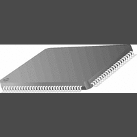
PC87393VJG National Semiconductor, PC87393VJG Datasheet - Page 31

PC87393VJG
Manufacturer Part Number
PC87393VJG
Description
IC, SUPER I/O DEVICE, TQFP-100
Manufacturer
National Semiconductor
Specifications of PC87393VJG
Data Rate
2Mbps
Supply Voltage Range
3V to 3.6V
Logic Case Style
TQFP
No. Of Pins
100
Operating Temperature Range
0°C to +70°C
Termination Type
SMD
Transceiver Type
Interface
Rohs Compliant
No
Available stocks
Company
Part Number
Manufacturer
Quantity
Price
Part Number:
PC87393VJG
Manufacturer:
NS/国半
Quantity:
20 000
- Current page: 31 of 148
- Download datasheet (2Mb)
2.0 Device Architecture and Configuration
2.2.4
SuperI/O Control and Configuration Registers
The SuperI/O configuration registers at indexes 20h and 27h are mainly used for part identification, global power manage-
ment and the selection of pin multiplexing options. For details, see Section 2.10.
Logical Device Control and Configuration Registers
A subset of these registers is implemented for each logical device. See functional block descriptions in the following sections.
Control
The only implemented control register for each logical device is the Activate register at index 30h. Bit 0 of the Activate reg-
ister controls the activation of the associated functional block. Activation enables access to the functional block’s registers,
and attaches its system resources, which are unassigned as long as it is not activated. Other effects may apply, on a func-
tion-specific basis (such as clock enable and active pinout signaling).
Standard Configuration
The standard configuration registers manage the PnP resource allocation to the functional blocks. The I/O port base address
descriptor 0 is a pair of registers at Index 60-61h, holding the first 16-bit base address for the register set of the functional
block. An optional 16-bit second base-address (descriptor 1) at index 62-63h is used for logical devices with more than one
Logical Device Control and
Configuration Registers -
SuperI/O Control and
Configuration Registers
one per Logical Device
(some are optional)
Standard Configuration Registers
2Bh - 2Eh
F0h - F9h
Figure 3. Configuration Register Map
Index
2Ah
07h
20h
21h
22h
23h
24h
25h
26h
27h
28h
29h
30h
60h
61h
70h
71h
74h
75h
Logical Device Number
SuperI/O ID
SuperI/O Configuration 1
SuperI/O Configuration 2
SuperI/O Configuration 3
SuperI/O Configuration 4
SuperI/O Configuration 5
SuperI/O Configuration 6
SuperI/O Revision ID
SuperI/O Configuration 8
SuperI/O Configuration 9
SuperI/O Configuration A
Reserved exclusively for National use
Logical Device Control (Activate)
I/O Base Address Descriptor 0 Bits 15-8
I/O Base Address Descriptor 0 Bits 7-0
Interrupt Number and Wake-Up on IRQ Enable
IRQ Type Select
DMA Channel Select 0
DMA Channel Select 1
Device Specific Logical Device Configuration 1 to 10
31
(Continued)
Register Name
www.national.com
Related parts for PC87393VJG
Image
Part Number
Description
Manufacturer
Datasheet
Request
R
Part Number:
Description:
National Semiconductor [8-Bit D/A Converter]
Manufacturer:
National Semiconductor
Datasheet:
Part Number:
Description:
National Semiconductor [Media Coprocessor]
Manufacturer:
National Semiconductor
Datasheet:
Part Number:
Description:
Digitally Controlled Tone and Volume Circuit with Stereo Audio Power Amplifier, Microphone Preamp Stage and National 3D Sound
Manufacturer:
National Semiconductor
Datasheet:
Part Number:
Description:
Digitally Controlled Tone and Volume Circuit with Stereo Audio Power Amplifier, Microphone Preamp Stage and National 3D Sound
Manufacturer:
National Semiconductor
Datasheet:
Part Number:
Description:
AC97 Rev 2 Codec with Sample Rate Conversion and National 3D Sound
Manufacturer:
National Semiconductor
Part Number:
Description:
Manufacturer:
National Semiconductor
Datasheet:
Part Number:
Description:
Manufacturer:
National Semiconductor
Datasheet:
Part Number:
Description:
General Purpose, Low Voltage, Low Power, Rail-to-Rail Output Operational Amplifiers
Manufacturer:
National Semiconductor
Datasheet:
Part Number:
Description:
8-bit 20 MSPS flash A/D converter.
Manufacturer:
National Semiconductor
Datasheet:
Part Number:
Description:
Low Noise Quad Operational Amplifier
Manufacturer:
National Semiconductor
Datasheet:
Part Number:
Description:
Quad Differential Line Receivers
Manufacturer:
National Semiconductor
Datasheet:
Part Number:
Description:
Quad High Speed Trapezoidal? Bus Transceiver
Manufacturer:
National Semiconductor
Datasheet:
Part Number:
Description:
Dual Line Receiver
Manufacturer:
National Semiconductor
Datasheet:
Part Number:
Description:
TTL to 10k ECL Level Translator with Latch
Manufacturer:
National Semiconductor
Datasheet:


