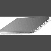
PC87393VJG National Semiconductor, PC87393VJG Datasheet - Page 28

PC87393VJG
Manufacturer Part Number
PC87393VJG
Description
IC, SUPER I/O DEVICE, TQFP-100
Manufacturer
National Semiconductor
Specifications of PC87393VJG
Data Rate
2Mbps
Supply Voltage Range
3V to 3.6V
Logic Case Style
TQFP
No. Of Pins
100
Operating Temperature Range
0°C to +70°C
Termination Type
SMD
Transceiver Type
Interface
Rohs Compliant
No
Available stocks
Company
Part Number
Manufacturer
Quantity
Price
Part Number:
PC87393VJG
Manufacturer:
NS/国半
Quantity:
20 000
- Current page: 28 of 148
- Download datasheet (2Mb)
www.national.com
2.0 Device Architecture and Configuration
2.2.2
Each functional block is associated with a Logical Device Number (LDN). The configuration registers are grouped into banks,
where each bank holds the standard configuration registers of the corresponding logical device. Table 6 shows the LDN
values of the PC8739x functional blocks. Any value not listed is reserved.
Figure 2 shows the structure of the standard configuration register file. The SuperI/O control and configuration registers are
not banked and are accessed by the Index-Data register pair only, as described above. However, the device control and
device configuration registers are duplicated over 9 banks for 9 logical devices. Therefore, accessing a specific register in
a specific bank is performed by two dimensional indexing, where the LDN register selects the bank (or logical device) and
the Index register selects the register within the bank. Accessing the Data register while the Index register holds a value of
30h or higher physically accesses the logical device configuration registers currently pointed to by the Index register, within
the logical device currently selected by the LDN register.
Write accesses to unimplemented registers (i.e. accessing the Data register while the Index register points to a non-existing
register), are ignored and read returns 00h on all addresses, except for 74h and 75h (DMA configuration registers) which
returns 04h (indicating no DMA channel is active). The configuration registers are accessible immediately after reset.
Banked Logical Device Registers Structure
LDN
(One per Logical Device)
0Ch
0Ah
0Bh
0Fh
00h
01h
02h
03h
07h
Floppy Disk Controller (FDC)
Parallel Port (PP)
Serial Port 2 with IR (SP2)
Serial Port 1 (SP1)
General-Purpose I/O (GPIO) Ports (PC87392, PC87393 and PC87393F only)
WATCHDOG Timer (WDT)
Game Port (GMP) (PC87393 and PC87393F only)
Musical Instrument Digital Interface (MIDI) Port (PC87393 and PC87393F only)
X-Bus Extension (PC87393 and PC87393F only)
Figure 2. Structure of Standard Configuration Register File
Table 6. Logical Device Number (LDN) Assignments
Banks
07h
20h
2Fh
30h
60h
63h
70h
71h
74h
75h
F0h
FEh
Logical Device Number Register
SuperI/O Configuration Registers
Logical Device Control Register
Standard Logical Device
Special (Vendor-defined)
Configuration Registers
Configuration Registers
Logical Device
Functional Block
28
(Continued)
Bank Select
Related parts for PC87393VJG
Image
Part Number
Description
Manufacturer
Datasheet
Request
R
Part Number:
Description:
National Semiconductor [8-Bit D/A Converter]
Manufacturer:
National Semiconductor
Datasheet:
Part Number:
Description:
National Semiconductor [Media Coprocessor]
Manufacturer:
National Semiconductor
Datasheet:
Part Number:
Description:
Digitally Controlled Tone and Volume Circuit with Stereo Audio Power Amplifier, Microphone Preamp Stage and National 3D Sound
Manufacturer:
National Semiconductor
Datasheet:
Part Number:
Description:
Digitally Controlled Tone and Volume Circuit with Stereo Audio Power Amplifier, Microphone Preamp Stage and National 3D Sound
Manufacturer:
National Semiconductor
Datasheet:
Part Number:
Description:
AC97 Rev 2 Codec with Sample Rate Conversion and National 3D Sound
Manufacturer:
National Semiconductor
Part Number:
Description:
Manufacturer:
National Semiconductor
Datasheet:
Part Number:
Description:
Manufacturer:
National Semiconductor
Datasheet:
Part Number:
Description:
General Purpose, Low Voltage, Low Power, Rail-to-Rail Output Operational Amplifiers
Manufacturer:
National Semiconductor
Datasheet:
Part Number:
Description:
8-bit 20 MSPS flash A/D converter.
Manufacturer:
National Semiconductor
Datasheet:
Part Number:
Description:
Low Noise Quad Operational Amplifier
Manufacturer:
National Semiconductor
Datasheet:
Part Number:
Description:
Quad Differential Line Receivers
Manufacturer:
National Semiconductor
Datasheet:
Part Number:
Description:
Quad High Speed Trapezoidal? Bus Transceiver
Manufacturer:
National Semiconductor
Datasheet:
Part Number:
Description:
Dual Line Receiver
Manufacturer:
National Semiconductor
Datasheet:
Part Number:
Description:
TTL to 10k ECL Level Translator with Latch
Manufacturer:
National Semiconductor
Datasheet:


