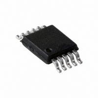
PCA9527DP,118 NXP Semiconductors, PCA9527DP,118 Datasheet - Page 9

PCA9527DP,118
Manufacturer Part Number
PCA9527DP,118
Description
IC BUFFER SHIFT DDC 3CH 10-TSSOP
Manufacturer
NXP Semiconductors
Type
Bufferr
Specifications of PCA9527DP,118
Tx/rx Type
I²C Logic
Delay Time
115ns
Capacitance - Input
8pF
Voltage - Supply
2.7 V ~ 5.5 V
Current - Supply
100mA
Mounting Type
Surface Mount
Package / Case
10-TSSOP
Operating Temperature (min)
-40C
Operating Temperature Classification
Industrial
Operating Temperature (max)
85C
Package Type
TSSOP
Rad Hardened
No
Logic Family
PCA
Number Of Channels Per Chip
3
Supply Voltage (max)
5.5 V
Supply Voltage (min)
2.7 V
Maximum Operating Temperature
+ 85 C
Mounting Style
SMD/SMT
Interface
DDC, I2C, SMBus
Minimum Operating Temperature
- 40 C
Propagation Delay Time
115 ns
Lead Free Status / RoHS Status
Lead free / RoHS Compliant
Other names
568-4770-2
Available stocks
Company
Part Number
Manufacturer
Quantity
Price
Company:
Part Number:
PCA9527DP,118
Manufacturer:
MAX
Quantity:
44
NXP Semiconductors
PCA9527_1
Product data sheet
Fig 7.
Sink or LCD TV application
RECEIVER
HDMI
3.3 V
(optional)
10 k
According to
I
the internal driver on port B to turn on, causing port B to pull down to about 0.5 V. When
port B of the PCA9527 falls, first a CMOS hysteresis type input detects the falling edge
and causes the internal driver on port A to turn on and pull the port A pin down to ground.
In order to illustrate what would be seen in a typical application, refer to
Figure
If the bus master in
shown in
transmission except that the HIGH level may be as low as 2.7 V, and the turn on and turn
off of the acknowledge signals are slightly delayed.
The master drives the B bus to ground or lets it float to V
at the falling edge of the 8
SDAA on the A bus to ground, causing the PCA9527 to pull SDAB on the B bus to 0.5 V.
At the falling edge of the 9
the A bus.
Multiple PCA9527 port A sides can be connected in a star configuration
allowing all nodes to communicate with each other.
Multiple PCA9527s can be connected in series
to port B. I
number of devices that can be connected in series is limited by repeater
delay/time-of-flight considerations on the maximum bus speed requirements.
2
C-bus, a comparator detects the falling edge when it goes below 0.3V
10 k
12.
10 k
Figure 11
2
C-bus slave devices can be connected to any of the bus segments. The
10 k
Figure
0.1 F
3-channel bidirectional bus extender for HDMI, I
SDAB
SCLB
CECB
EN
would be observed on the A bus. This looks like a normal I
V
Figure 5
5, when port A of the PCA9527 is pulled LOW by a driver on the
CC(B)
PCA9527
Rev. 01 — 29 June 2009
GND
th
th
V
clock, master releases SDAB on the B bus and slave pulls
clock, the master again drives the B bus and slave releases
CC(A)
were to write to the slave through the PCA9527, waveforms
SDAA
SCLA
CECA
0.1 F
10 k
47 k
(Figure
LCD TV
22
22
5 V
9) as long as port A is connected
CC(B)
HDMI cable
DDC line
as it sends data to the slave
2
PCA9527
C-bus and SMBus
© NXP B.V. 2009. All rights reserved.
CC(A)
DVD (source)
Figure 11
PCA9512A
(Figure
PCA9507
PCA9515
PCA9517
PCA9527
002aad973
and causes
2
C-bus
8),
and
9 of 22


