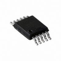
PCA9527DP,118 NXP Semiconductors, PCA9527DP,118 Datasheet - Page 4

PCA9527DP,118
Manufacturer Part Number
PCA9527DP,118
Description
IC BUFFER SHIFT DDC 3CH 10-TSSOP
Manufacturer
NXP Semiconductors
Type
Bufferr
Specifications of PCA9527DP,118
Tx/rx Type
I²C Logic
Delay Time
115ns
Capacitance - Input
8pF
Voltage - Supply
2.7 V ~ 5.5 V
Current - Supply
100mA
Mounting Type
Surface Mount
Package / Case
10-TSSOP
Operating Temperature (min)
-40C
Operating Temperature Classification
Industrial
Operating Temperature (max)
85C
Package Type
TSSOP
Rad Hardened
No
Logic Family
PCA
Number Of Channels Per Chip
3
Supply Voltage (max)
5.5 V
Supply Voltage (min)
2.7 V
Maximum Operating Temperature
+ 85 C
Mounting Style
SMD/SMT
Interface
DDC, I2C, SMBus
Minimum Operating Temperature
- 40 C
Propagation Delay Time
115 ns
Lead Free Status / RoHS Status
Lead free / RoHS Compliant
Other names
568-4770-2
Available stocks
Company
Part Number
Manufacturer
Quantity
Price
Company:
Part Number:
PCA9527DP,118
Manufacturer:
MAX
Quantity:
44
NXP Semiconductors
6. Functional description
PCA9527_1
Product data sheet
Table 2.
Refer to
The PCA9527 consists of 3 channels of bidirectional open-drain I/Os specifically designed
to support up-translation/down-translation between low voltages (as low as 2.7 V) and a
3.3 V or 5 V I
on port A of the SCLA and SDAA that enables the device to drive a long cable or a heavier
capacitive load for DDC, I
device translates from voltage ranges 2.7 V to 5.5 V down to a voltage as low as 2.7 V
without degradation of system performance. Unlike the SDAA and SCLA, the CECA is
powered by the V
port A has normal I/O and port B static level offset. All I/Os are overvoltage tolerant to
5.5 V even when the device is un-powered (V
The PCA9527 includes a power-up circuit that keeps the SDA and SCL output drivers
turned off until V
OFF until V
power-up.
When port B falls first and goes below 0.3V
pulls down to 0 V. As port A falls below 0.3V
The external port B driver must drive the port B to a LOW that is
possible to know who is driving the port A LOW. The PCA9527 direction control assumes
that port A is controlling the part unless port B falls below 0.4 V. When the port B voltage
is
the port B voltage rises because the external driver turns off, the port B voltage rises up to
~0.5 V because port A is LOW; once port B rises to ~0.5 V the port A pull-down driver
turns off. Then port A rises with a rise time determined by the RC of port A when it
Symbol
GND
EN
CECB
SDAB
SCLB
V
Fig 3.
CC(B)
0.4 V the port A driver of the PCA9527 is on and holds port A down to nearly 0 V. As
Figure 1 “Functional diagram of
Port A and port B I/O levels
Pin description
CC(B)
Pin
5
6
7
8
9
10
2
C-bus and SMBus. The device contains a rise time accelerator, specifically
CC(A)
rises above 2.7 V. V
CC(B)
3-channel bidirectional bus extender for HDMI, I
Description
supply ground (0 V)
active HIGH buffer enable input
serial data with static level offset, powered by V
serial data port B bus with static level offset, 5 V tolerant
serial clock port B bus with static level offset, 5 V tolerant
port B supply voltage (2.7 V to 3.6 V)
and V
and does not have a rise time accelerator, but is similar in that its
Rev. 01 — 29 June 2009
V
V
0.3V
CC(B)
CC(A)
2
…continued
C-bus and SMBus applications. With dual supply rails, the
0.3V
CC(B)
CC(B)
CC(A)
rise above 2.7 V. The CECA output drivers are turned
0.4 V
CC(A)
port B
port A
PCA9527”.
and V
CC(B)
CC(A)
CC(B)
CC(B)
the port A driver is turned on and port A
the port B pulls down to about 0.5 V.
0.5 V
and/or V
can be applied in any sequence at
0.7V
002aad435
CC(A)
CC(A)
CC(B)
0 V
0 V
= 0 V).
, 5 V tolerant
0.4 V or else it is not
2
PCA9527
C-bus and SMBus
© NXP B.V. 2009. All rights reserved.
4 of 22


