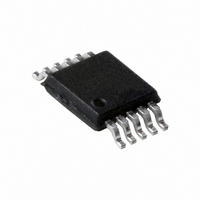
PCA9527DP,118 NXP Semiconductors, PCA9527DP,118 Datasheet - Page 7

PCA9527DP,118
Manufacturer Part Number
PCA9527DP,118
Description
IC BUFFER SHIFT DDC 3CH 10-TSSOP
Manufacturer
NXP Semiconductors
Type
Bufferr
Specifications of PCA9527DP,118
Tx/rx Type
I²C Logic
Delay Time
115ns
Capacitance - Input
8pF
Voltage - Supply
2.7 V ~ 5.5 V
Current - Supply
100mA
Mounting Type
Surface Mount
Package / Case
10-TSSOP
Operating Temperature (min)
-40C
Operating Temperature Classification
Industrial
Operating Temperature (max)
85C
Package Type
TSSOP
Rad Hardened
No
Logic Family
PCA
Number Of Channels Per Chip
3
Supply Voltage (max)
5.5 V
Supply Voltage (min)
2.7 V
Maximum Operating Temperature
+ 85 C
Mounting Style
SMD/SMT
Interface
DDC, I2C, SMBus
Minimum Operating Temperature
- 40 C
Propagation Delay Time
115 ns
Lead Free Status / RoHS Status
Lead free / RoHS Compliant
Other names
568-4770-2
Available stocks
Company
Part Number
Manufacturer
Quantity
Price
Company:
Part Number:
PCA9527DP,118
Manufacturer:
MAX
Quantity:
44
NXP Semiconductors
PCA9527_1
Product data sheet
6.3.3 Port B (SDAB, SCLB, CECB)
SDAB and SCLB are standard I
accelerator. The static level offset produces an output LOW of 0.5 V (typical) at 6 mA. As
with the standard I
levels. The size of these pull-up resistors depends on the system requirement, and should
meet the current sinking capability of the device that drives the buffer, as well as that of
the buffer. The minimum and maximum pull-up resistors are determined and the pull-up
resistor’s value is chosen to be within the minimum and maximum range.
Using
R
Where:
The maximum pull-up resistor should also be sized such that the RC time constant meets
the standard I
Fast-mode (400 kHz). DDC bus complies with the I
below 100 kHz, and maximum rise time is 1 s using a simplified RC equation.
Using
Where:
The chosen pull-up resistor R
R
PU min
PU max
R
V
0.4 V is the maximum V
I
on logic LOW.
R
meet the I
C
the line, and the buffer) in order to meet the rise time specification.
t
speed 400 kHz or lower).
OL(max)
r
pu(max)
PU(min)
PU(max)
L(max)
is the rise time specified as 1 s (for bus speed 100 kHz or lower) and 300 ns (for bus
Equation
Equation
=
is the maximum allowable capacitance load (include the capacitance of driver,
at V
is the maximum supply rail of the pull-up resistor and should not exceed 5.5 V.
is the minimum pull-up resistor value for the open-drain SCLB and SDAB.
is the maximum allowable pull-up resistor on the SCLB and SDAB in order to
C
V
---------------------------------------- -
2
L max
C-bus rise time specification.
pu max
2
OL
C-bus rise time, which is 1 s for Standard-mode (100 kHz) or 300 ns for
I
1, calculate the minimum pull-up resistor value:
2, calculate the maximum pull-up resistor value:
OL max
= 0.4 V is the maximum sink current of the device that drives the buffer
3-channel bidirectional bus extender for HDMI, I
2
C-bus system, pull-up resistors are required to provide the logic HIGH
=
–
1.2 t
0.4 V
Rev. 01 — 29 June 2009
OL
r
of the device that drives the buffer on logic LOW.
PU
2
C-bus with static level offset that has no rise time
is: R
PU(min)
R
PU
2
C-bus Standard-mode and operates
R
PU(max)
.
2
PCA9527
C-bus and SMBus
© NXP B.V. 2009. All rights reserved.
7 of 22
(1)
(2)


