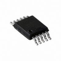
PCA9527DP,118 NXP Semiconductors, PCA9527DP,118 Datasheet - Page 5

PCA9527DP,118
Manufacturer Part Number
PCA9527DP,118
Description
IC BUFFER SHIFT DDC 3CH 10-TSSOP
Manufacturer
NXP Semiconductors
Type
Bufferr
Specifications of PCA9527DP,118
Tx/rx Type
I²C Logic
Delay Time
115ns
Capacitance - Input
8pF
Voltage - Supply
2.7 V ~ 5.5 V
Current - Supply
100mA
Mounting Type
Surface Mount
Package / Case
10-TSSOP
Operating Temperature (min)
-40C
Operating Temperature Classification
Industrial
Operating Temperature (max)
85C
Package Type
TSSOP
Rad Hardened
No
Logic Family
PCA
Number Of Channels Per Chip
3
Supply Voltage (max)
5.5 V
Supply Voltage (min)
2.7 V
Maximum Operating Temperature
+ 85 C
Mounting Style
SMD/SMT
Interface
DDC, I2C, SMBus
Minimum Operating Temperature
- 40 C
Propagation Delay Time
115 ns
Lead Free Status / RoHS Status
Lead free / RoHS Compliant
Other names
568-4770-2
Available stocks
Company
Part Number
Manufacturer
Quantity
Price
Company:
Part Number:
PCA9527DP,118
Manufacturer:
MAX
Quantity:
44
NXP Semiconductors
PCA9527_1
Product data sheet
6.3.1 Port A (SDAA and SCLA)
6.1 Enable
6.2 Rise time accelerators
6.3 Resistor pull-up value selection
crosses the port A threshold ~0.3V
accelerator is turned on, which causes a faster rising edge until it reaches the turn-off
point for the rising edge accelerator ~0.7V
determined by the RC of port A. When the port B driver turns off, port B rises with the RC
of port B.
V
good detect circuit. V
I/Os, and the support functions.
and port B.
The EN pin is active HIGH with an internal ~100 k pull-up to V
to select when the buffer is active. The enable pin puts the PCA9527 in a power-down
state when it is disabled, so that there is a recovery delay and a lower power-down power.
This can be used to isolate the line when the HDMI DDC transmitter or receiver is not
ready, or from a badly behaved slave on power-up until after the system power-up reset. It
should never change state during an I
operation will hang the bus and enabling part way through a bus cycle could confuse the
I
bus and the buffer port are in an idle state to prevent system failures.
PCA9527 has rise time accelerators on port A of SCL and SDA only; the CECA pin does
not have a rise time accelerator. During port A positive bus transitions a current source is
switched on to quickly slew the SDAA and SCLA lines HIGH once the input level of
0.3V
approached.
SDAA and SCLA are open-drain I/O that have rise time accelerators and strong pull-down.
When the inputs transition above 0.3V
the pull-up current during rising edge to meet the I
device drives a long cable or heavier capacitance load. The strong pull-down enables the
output to drive to nearly zero voltage for logic LOW. The selection for pull-up resistors are
defined in the HDMI DDC specification shown in
applications like digital video player, recorder, or set-top box, the pull-up resistor is in the
range of 1.5 k to 2 k . For HDMI receiver applications like in LCD TV or video card, the
pull-up resistor is 47 k on the SCLA line, and there is no pull-up on the SDAA line.
Please refer to
pull-up resistor values (in k ) versus capacitance load (in nF) for 5 V supply voltage
complied with 1 s rise time per I
contrasts a shaded and unshaded region. Any resistor value chosen within the unshaded
region would comply with 1 s rise time, while any value chosen in the shaded region
would not.
2
CC(A)
C-bus parts being enabled. The enable pin should only change state when the global
CC(A)
powers the 0.3V
is exceeded for the PCA9527 and turns off as the 0.7V
Table
3-channel bidirectional bus extender for HDMI, I
CC(B)
3,
CC(A)
Rev. 01 — 29 June 2009
Figure 6
powers the rest of the chip including the port B I/Os, the CEC
reference for SCLA and SDAA as well as the port A power
Figure 3
and
2
C-bus Standard-mode specification. The graph
CC(A)
Figure 7
2
CC(A)
C-bus operation because disabling during a bus
the port B driver is turned off and the rising edge
illustrates the threshold and I/O levels for port A
CC(A)
, the rise time accelerator activates and boosts
for more details.
. Then it continues to rise at the slower rate
Table
2
C-bus rise time specification when the
3. For HDMI transmitter
Figure 4
CC(B)
CC(A)
and allows the user
2
PCA9527
C-bus and SMBus
voltage is
© NXP B.V. 2009. All rights reserved.
shows the port A
5 of 22


