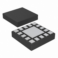
PCA9574HR,115 NXP Semiconductors, PCA9574HR,115 Datasheet - Page 6

PCA9574HR,115
Manufacturer Part Number
PCA9574HR,115
Description
IC I/O EXPANDER I2C 8B 16HXQFN
Manufacturer
NXP Semiconductors
Datasheet
1.PCA9574HR115.pdf
(32 pages)
Specifications of PCA9574HR,115
Interface
I²C, SMBus
Number Of I /o
8
Interrupt Output
Yes
Frequency - Clock
400kHz
Voltage - Supply
1.1 V ~ 3.6 V
Operating Temperature
-40°C ~ 85°C
Mounting Type
Surface Mount
Package / Case
16-XQFN (Exposed Pad), 16-eXQFN, 16-HXQFN
Includes
POR
Logic Family
CMOS
Number Of Lines (input / Output)
8 / 8
Operating Supply Voltage
1.1 V to 3.6 V
Power Dissipation
75 mW
Operating Temperature Range
- 40 C to + 85 C
Input Voltage
1.1 V to 4.1 V
Logic Type
I2C Bus Extender
Maximum Clock Frequency
400 KHz
Maximum Operating Frequency
400 KHz
Mounting Style
SMD/SMT
Number Of Input Lines
8
Number Of Output Lines
8
Output Current
+/- 5 mA
Output Voltage
1.1 V to 4.1 V
Lead Free Status / RoHS Status
Lead free / RoHS Compliant
Lead Free Status / RoHS Status
Lead free / RoHS Compliant, Lead free / RoHS Compliant
Other names
568-4936-2
NXP Semiconductors
7. Functional description
PCA9574_2
Product data sheet
6.2 Pin description
7.1 Device address
Table 3.
[1]
Following a START condition the bus master must send the address of the slave it is
accessing and the operation it wants to perform (read or write). The address of the
PCA9574 is shown in
or 42h.
The last bit of the first byte defines the operation to be performed. When set to logic 1 a
read is selected, while logic 0 selects a write operation.
Symbol
INT
A0
RESET
P0
P1
P2
P3
V
V
P4
P5
P6
P7
SCL
SDA
V
Fig 6.
SS
DD(IO)
DD
HVQFN16, HXQFN16U package die supply ground is connected to both V
V
and board level performance, the exposed pad needs to be soldered to the board using a corresponding
thermal pad on the board and for proper heat conduction through the board, thermal vias need to be
incorporated in the PCB in the thermal pad region.
SS
pin must be connected to supply ground for proper device operation. For enhanced thermal, electrical,
PCA9574 device address
Pin
TSSOP16 HVQFN16 HXQFN16U
1
2
3
4
5
6
7
8
9
10
11
12
13
14
15
16
Pin description
15
16
1
2
3
4
5
6
7
8
9
10
11
12
13
14
Figure
[1]
Rev. 02 — 27 July 2009
8-bit I
0
6. Slave address pin A0 chooses 1 of 2 slave addresses: 40h
1
2
C-bus and SMBus, level translating, low voltage GPIO
14
15
16
1
2
3
4
5
6
7
8
9
10
11
12
13
[1]
slave address
0
fixed
0
0
Type
O
I
I
I/O
I/O
I/O
I/O
ground
power supply
I/O
I/O
I/O
I/O
I
I/O
power supply
0
A0 R/W
hardware selectable
002aad055
Description
active LOW interrupt output;
active LOW SMBus alert output
address input
active LOW reset input
input/output 0
input/output 1
input/output 2
input/output 3
supply ground
I/O bank supply voltage
input/output 4
input/output 5
input/output 6
input/output 7
serial clock line
serial data line
supply voltage
SS
pin and exposed center pad.
PCA9574
© NXP B.V. 2009. All rights reserved.
6 of 32


