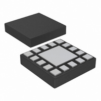
PCA9574HR,115 NXP Semiconductors, PCA9574HR,115 Datasheet - Page 13

PCA9574HR,115
Manufacturer Part Number
PCA9574HR,115
Description
IC I/O EXPANDER I2C 8B 16HXQFN
Manufacturer
NXP Semiconductors
Datasheet
1.PCA9574HR115.pdf
(32 pages)
Specifications of PCA9574HR,115
Interface
I²C, SMBus
Number Of I /o
8
Interrupt Output
Yes
Frequency - Clock
400kHz
Voltage - Supply
1.1 V ~ 3.6 V
Operating Temperature
-40°C ~ 85°C
Mounting Type
Surface Mount
Package / Case
16-XQFN (Exposed Pad), 16-eXQFN, 16-HXQFN
Includes
POR
Logic Family
CMOS
Number Of Lines (input / Output)
8 / 8
Operating Supply Voltage
1.1 V to 3.6 V
Power Dissipation
75 mW
Operating Temperature Range
- 40 C to + 85 C
Input Voltage
1.1 V to 4.1 V
Logic Type
I2C Bus Extender
Maximum Clock Frequency
400 KHz
Maximum Operating Frequency
400 KHz
Mounting Style
SMD/SMT
Number Of Input Lines
8
Number Of Output Lines
8
Output Current
+/- 5 mA
Output Voltage
1.1 V to 4.1 V
Lead Free Status / RoHS Status
Lead free / RoHS Compliant
Lead Free Status / RoHS Status
Lead free / RoHS Compliant, Lead free / RoHS Compliant
Other names
568-4936-2
NXP Semiconductors
8. Characteristics of the I
PCA9574_2
Product data sheet
7.10 Standby
7.9 Interrupt output (INT)
8.1 Bit transfer
The open-drain active LOW interrupt is activated when one of the port pins changes state
and the port pin is configured as an input and the interrupt on it is not masked. The
interrupt is deactivated when the port pin input returns to its previous state or the Input
Port register is read. It is highly recommended to program the MSK register, and the CFG
registers during the initialization sequence after power-up, since any change to them
during Normal mode operation may cause undesirable interrupt events to happen.
Remark: Changing an I/O from an output to an input may cause a false interrupt to occur
if the state of the pin does not match the contents of the Input port register. Only a read of
the Input port register that contains the bit(s) image of the input(s) that generated the
interrupt clears the interrupt condition.
The PCA9574 goes into standby when the I
than 1.0 A (typical).
The I
lines are a serial data line (SDA) and a serial clock line (SCL). Both lines must be
connected to a positive supply via a pull-up resistor when connected to the output stages
of a device. Data transfer may be initiated only when the bus is not busy.
One data bit is transferred during each clock pulse. The data on the SDA line must remain
stable during the HIGH period of the clock pulse as changes in the data line at this time
will be interpreted as control signals (see
5. Once the right byte has been sent and correctly acknowledged, the master sends a
Fig 8.
STOP command to end the Software Reset sequence: the PCA9574 then resets to
the default value (power-up value) and is ready to be addressed again within the
specified bus free time. If the master sends a Repeated START instead, no reset is
performed. The I
(at any time) as a ‘Software Reset Abort’. The PCA9574 does not initiate a software
reset.
2
C-bus is for 2-way, 2-line communication between different ICs or modules. The two
Bit transfer
2
SDA
SCL
C-bus
2
C-bus master must interpret a non-acknowledge from the PCA9574
Rev. 02 — 27 July 2009
8-bit I
2
C-bus and SMBus, level translating, low voltage GPIO
data valid
data line
stable;
Figure
2
C-bus is idle. Standby supply current is lower
allowed
change
of data
8).
mba607
PCA9574
© NXP B.V. 2009. All rights reserved.
13 of 32


