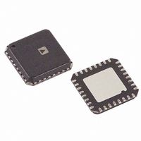
ADV7391BCPZ Analog Devices Inc, ADV7391BCPZ Datasheet - Page 52

ADV7391BCPZ
Manufacturer Part Number
ADV7391BCPZ
Description
IC ENCODER VIDEO W/DAC 32-LFCSP
Manufacturer
Analog Devices Inc
Type
Video Encoderr
Datasheet
1.ADV7393BCPZ.pdf
(108 pages)
Specifications of ADV7391BCPZ
Applications
Set-Top Boxes, Video Players, Displays
Voltage - Supply, Analog
2.6 V ~ 3.46 V
Voltage - Supply, Digital
1.71 V ~ 1.89 V
Mounting Type
Surface Mount
Package / Case
32-LFCSP
Supply Voltage Range
1.71V To 1.89V
Operating Temperature Range
-40°C To +85°C
Tv / Video Case Style
LFCSP
No. Of Pins
32
Svhc
No SVHC (18-Jun-2010)
Operating Temperature Max
85°C
Operating
RoHS Compliant
Input Format
Digital
Output Format
Analogue
Dac Resolution
10bit
Rohs Compliant
Yes
Lead Free Status / RoHS Status
Lead free / RoHS Compliant
For Use With
EVAL-ADV7391EBZ - BOARD EVAL FOR ADV7391 ENCODER
Lead Free Status / RoHS Status
Lead free / RoHS Compliant
Available stocks
Company
Part Number
Manufacturer
Quantity
Price
Company:
Part Number:
ADV7391BCPZ
Manufacturer:
CIRRUS
Quantity:
7 400
Company:
Part Number:
ADV7391BCPZ
Manufacturer:
ADI
Quantity:
302
Part Number:
ADV7391BCPZ
Manufacturer:
ADI/亚德诺
Quantity:
20 000
Company:
Part Number:
ADV7391BCPZ-3
Manufacturer:
AD
Quantity:
1 831
Company:
Part Number:
ADV7391BCPZ-REEL
Manufacturer:
HIT
Quantity:
530
Part Number:
ADV7391BCPZ-REEL
Manufacturer:
ADI/亚德诺
Quantity:
20 000
ADV7390/ADV7391/ADV7392/ADV7393
In SD Timing Mode 0 (slave option), if VBI is enabled, the
blanking bit in the EAV/SAV code is overwritten. It is possible
to use VBI in this timing mode as well.
If CGMS is enabled and VBI is disabled, the CGMS data is,
nevertheless, available at the output.
SD SUBCARRIER FREQUENCY CONTROL
Subaddress 0x8C to Subaddress 0x8F
The ADV739x is able to generate the color subcarrier used in
CVBS and S-Video (Y-C) outputs from the input pixel clock.
Four 8-bit registers are used to set up the subcarrier frequency.
The value of these registers is calculated using the following
equation:
where the sum is rounded to the nearest integer.
For example, in NTSC mode:
where:
Subcarrier Register Value = 569408543d = 0×21F07C1F
SD F
SD F
SD F
SD F
Programming the F
The subcarrier frequency register value is divided into four F
registers as shown in the previous example. The four subcarrier
frequency registers must be updated sequentially, starting with
Subcarrier Frequency Register 0 and ending with Subcarrier
Frequency Register 3. The subcarrier frequency updates only
after the last subcarrier frequency register byte is received by
the ADV739x. The SD input standard autodetection feature
must be disabled.
Typical F
Table 42 outlines the values that should be written to the
subcarrier frequency registers for NTSC and PAL B/D/G/H/I.
SC
SC
SC
SC
Subcarrier
Subcarrier
Number
Number
Register 0: 0x1F
Register 1: 0x7C
Register 2: 0xF0
Register 3: 0x21
SC
Values
of
of
Frequency
Register
27
subcarrier
MHz
SC
Value
clock
Register
periods
=
cycles
⎛
⎜
⎝
227
1716
=
in
in
5 .
one
one
⎞
⎟
⎠
×
video
2
video
32
=
line
569408543
line
×
2
32
Rev. B | Page 52 of 108
SC
Table 42. Typical F
Subaddress
0x8C
0x8D
0x8E
0x8F
SD NONINTERLACED MODE
Subaddress 0x88, Bit 1
The ADV739x supports an SD noninterlaced mode. Using this
mode, progressive inputs at twice the frame rate of NTSC and
PAL (240p/59.94 Hz and 288p/50 Hz, respectively) can be input
into the ADV739x. The SD noninterlaced mode can be enabled
using Subaddress 0x88, Bit 1.
A 27 MHz clock signal must be provided on the CLKIN pin.
Embedded EAV/SAV timing codes or external horizontal and
vertical synchronization signals provided on the HSYNC and
VSYNC pins can be used to synchronize the input pixel data.
All input configurations, output configurations, and features
available in NTSC and PAL modes are available in SD noninter-
laced mode. For 240p/59.94 Hz input, the ADV739x should be
configured for NTSC operation and Subaddress 0x88, Bit 1
should be set to 1.
For 288p/50 Hz input, the ADV739x should be configured for
PAL operation and Subaddress 0x88, Bit 1 should be set to 1.
SD SQUARE PIXEL MODE
Subaddress 0x82, Bit 4
The ADV739x supports an SD square pixel mode (Subaddress
0x82, Bit 4). For NTSC operation, an input clock of 24.5454 MHz
is required. The active resolution is 640 × 480. For PAL
operation, an input clock of 29.5 MHz is required. The active
resolution is 768 × 576.
For CVBS and S-Video (Y-C) outputs, the SD subcarrier
frequency registers must be updated to reflect the input clock
frequency used in SD square pixel mode. The SD input standard
autodetection feature must be disabled in SD square pixel
mode. In square pixel mode, the timing diagrams shown in
Figure 67 and Figure 68 apply.
Description
F
F
F
F
SC
SC
SC
SC
SC
0
1
2
3
Values
NTSC
0x1F
0x7C
0xF0
0x21
PAL B/D/G/H/I
0xCB
0x8A
0x09
0x2A


