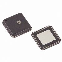
ADV7391BCPZ Analog Devices Inc, ADV7391BCPZ Datasheet - Page 45

ADV7391BCPZ
Manufacturer Part Number
ADV7391BCPZ
Description
IC ENCODER VIDEO W/DAC 32-LFCSP
Manufacturer
Analog Devices Inc
Type
Video Encoderr
Datasheet
1.ADV7393BCPZ.pdf
(108 pages)
Specifications of ADV7391BCPZ
Applications
Set-Top Boxes, Video Players, Displays
Voltage - Supply, Analog
2.6 V ~ 3.46 V
Voltage - Supply, Digital
1.71 V ~ 1.89 V
Mounting Type
Surface Mount
Package / Case
32-LFCSP
Supply Voltage Range
1.71V To 1.89V
Operating Temperature Range
-40°C To +85°C
Tv / Video Case Style
LFCSP
No. Of Pins
32
Svhc
No SVHC (18-Jun-2010)
Operating Temperature Max
85°C
Operating
RoHS Compliant
Input Format
Digital
Output Format
Analogue
Dac Resolution
10bit
Rohs Compliant
Yes
Lead Free Status / RoHS Status
Lead free / RoHS Compliant
For Use With
EVAL-ADV7391EBZ - BOARD EVAL FOR ADV7391 ENCODER
Lead Free Status / RoHS Status
Lead free / RoHS Compliant
Available stocks
Company
Part Number
Manufacturer
Quantity
Price
Company:
Part Number:
ADV7391BCPZ
Manufacturer:
CIRRUS
Quantity:
7 400
Company:
Part Number:
ADV7391BCPZ
Manufacturer:
ADI
Quantity:
302
Part Number:
ADV7391BCPZ
Manufacturer:
ADI/亚德诺
Quantity:
20 000
Company:
Part Number:
ADV7391BCPZ-3
Manufacturer:
AD
Quantity:
1 831
Company:
Part Number:
ADV7391BCPZ-REEL
Manufacturer:
HIT
Quantity:
530
Part Number:
ADV7391BCPZ-REEL
Manufacturer:
ADI/亚德诺
Quantity:
20 000
ADV7390/ADV7391 INPUT CONFIGURATION
The ADV7390/ADV7391 support a number of different input
modes. The desired input mode is selected using Subaddress 0x01,
Bits[6:4]. The ADV7390/ADV7391 default to standard definition
(SD) mode on power-up. Table 35 provides an overview of all
possible input configurations. Each input mode is described in
detail in this section. Note that the WLCSP option is only
configured to support SD as shown in Figure 51.
Table 35. ADV7390/ADV7391 Input Configuration
Input Mode
000
010
111
STANDARD DEFINITION
Subaddress 0x01, Bits[6:4] = 000
SD YCrCb data can be input in an interleaved 4:2:2 format over
an 8-bit bus rate of 27 MHz. A 27 MHz clock signal must be
provided on the CLKIN pin. If required, external synchroni-
zation signals can be provided on the HSYNC and VSYNC pins.
Embedded EAV/SAV timing codes are also supported. The
ITU-R BT.601/656 input standard is supported. The interleaved
pixel data is input on Pin P7 to Pin P0, with Pin P0 being the LSB.
ENHANCED DEFINITION/HIGH DEFINITION
Subaddress 0x01, Bits[6:4] = 010
Enhanced definition (ED) or high definition (HD) YCrCb data
can be input in an interleaved 4:2:2 format over an 8-bit DDR
bus. The clock signal must be provided on the CLKIN pin. If
required, external synchronization signals can be provided on
the HSYNC and VSYNC pins. Embedded EAV/SAV timing
codes are also supported.
8-Bit 4:2:2 ED/HD YCrCb Mode (DDR)
In 8-bit DDR 4:2:2 YCrCb input mode, the Y pixel data is input
on Pin P7 to Pin P0 on either the rising or falling edge of CLKIN.
Pin P0 is the LSB.
SD
ED (at 54 MHz)
ED/HD-DDR
DECODER
MPEG2
YCrCb
Figure 51. SD Example Application
P7
27MHz
2
8
P6
P5
CLKIN
P[7:0]
HSYNC
VSYNC,
ADV7390/
ADV7391
P4
YCrCb
YCrCb
YCrCb
P3
P2
P1
Rev. B | Page 45 of 108
P0
The CrCb pixel data is also input on Pin P7 to Pin P0 on the
opposite edge of CLKIN. Pin P0 is the LSB.
Whether the Y data is clocked in on the rising or falling edge of
CLKIN is determined by Subaddress 0x01, Bits[2:1] (see Figure 52
and Figure 53).
ENHANCED DEFINITION (AT 54 MHz)
Subaddress 0x01, Bits[6:4] = 111
ED YCrCb data can be input in an interleaved 4:2:2 format over
an 8-bit bus rate of 54 MHz.
A 54 MHz clock signal must be provided on the CLKIN pin.
Embedded EAV/SAV timing codes are supported. External
synchronization signals are not supported in this mode.
The interleaved pixel data is input on Pin P7 to Pin P0, with Pin P0
being the LSB.
NOTES
1. SUBADDRESS 0x01 [2:1] SHOULD BE SET TO 11 IN THIS CASE.
CLKIN
P[7:0]
NOTES
1. SUBADDRESS 0x01 [2:1] SHOULD BE SET TO 00 IN THIS CASE.
CLKIN
ADV7390/ADV7391/ADV7392/ADV7393
P[7:0]
CLKIN
P[7:0]
Figure 52. ED/HD-DDR Input Sequence (EAV/SAV)—Option A
Figure 53. ED/HD-DDR Input Sequence (EAV/SAV)—Option B
3FF
Figure 55. ED (at 54 MHz) Input Sequence (EAV/SAV)
3FF
INTERLACED TO
3FF
PROGRESSIVE
DECODER
Figure 54. ED/HD-DDR Example Application
MPEG2
YCrCb
00
00
00
00
00
00
YCrCb
XY
XY
2
XY
8
Cb0
Cb0
Y0
CLKIN
P[7:0]
VSYNC,
HSYNC
ADV7390/
ADV7391
Y0
Y0
Cb0
Cr0
Cr0
Y1
Y1
Y1
Cr0


