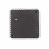
DP83907VF National Semiconductor, DP83907VF Datasheet - Page 53

DP83907VF
Manufacturer Part Number
DP83907VF
Description
IC CONTROLLR AT/LANII TP 160PQFP
Manufacturer
National Semiconductor
Datasheet
1.DP83907VF.pdf
(70 pages)
Specifications of DP83907VF
Controller Type
Network Interface Controller (NIC)
Interface
Twisted Pair
Voltage - Supply
4.75 V ~ 5.25 V
Current - Supply
150mA
Operating Temperature
0°C ~ 70°C
Mounting Type
Surface Mount
Package / Case
160-MQFP, 160-PQFP
Lead Free Status / RoHS Status
Contains lead / RoHS non-compliant
Other names
*DP83907VF
Available stocks
Company
Part Number
Manufacturer
Quantity
Price
Company:
Part Number:
DP83907VF
Manufacturer:
NSC
Quantity:
5 510
6 0 Operation of DP83907
The DMA Address will be incremented and the Byte Coun-
ter will be decremented after each transjer The DMA is
terminated when the Remote Byte Count Register reaches
zero
Send Packet Command The Remote DMA channel can
be automatically initialized to transfer a single packet from
the Receive Buffer Ring The CPU begins this transfer by
issuing a ‘‘Send Packet’’ Command The DMA will be initial-
ized to the value of the Boundary Pointer Register and the
Remote Byte Count Register pair (RBCR0 RBCR1) will be
initialized to the value of the Receive Byte Count fields
found in the Buffer Header of each packet After the data is
transferred the Boundary Pointer is advanced to allow the
buffers to be used for new receive packets The Remote
Read will terminate when the Byte Count equals zero The
Remote DMA is then prepared to read the next packet from
the Receive Buffer Ring If the DMA pointer crosses the
Page Stop Register it is reset to the Page Start Address
This allows the Remote DMA to remove packets that have
wrapped around to the top of the Receive Buffer Ring
Note 1 In order for the DP83907 Controller to correctly execute the Send
Note 2 The Send Packet command cannot be used with 680x0 type proc-
I O READ TIMlNG
1) The DMA reads word from local buffer memory and
2) Internally a request line is asserted to enable the system
3) The system reads the port the read strobe for the port is
Steps 1 –3 are repeated until the remote DMA is complete
(i e the byte count has gone to zero )
Note that in order for the Remote DMA to transfer a word
from memory to the latch it must arbitrate access to the
local buffer RAM After each word is transferred to the inter-
nal latch access to the RAM is relinquished If a Local DMA
is in progress the Remote DMA is held off until the local
DMA is complete
writes the word into the internal latch increments the
DMA
(RBCR0 1)
to read the port If the system reads this port before the
data has been written then the system is sent a wait
signal to wait until the data has been written to the port
Once written the systems read is allowed to complete
used as an acknowledge to the Remote DMA and it goes
back to step 1
Packet Command the upper Remote Byte Count Register (RBCR1)
must first be loaded with 0FH
essors
address
and
decrements
the
(Continued)
byte
count
53
I O WRITE TIMING
A Remote Write operation transfers data from the I O port
to the local buffer RAM The system transfers a byte-word
to the latch via IOWR This write strobe is detected by the
DP83907 and the byte word is transferred to local buffer
memory The Remote DMA holds off further transfers into
the latch until the current byte word has been transferred
from the latch
1) DP83907 awaits data to be written by the system Sys-
2) Remote DMA reads contents of port and writes byte
3) Go back to step 1
6 7 FUNCTIONAL BUS TIMING
This section describes the bus cycles that the DP83907 per-
forms These timings can be subdivided into 3 basic catego-
ries
1 ISA I O Access There are register accesses in both
2 Shared RAM ISA Accesses These are the timing for the
3 Boot PROM ISA Accesses These are the timing for the
4 Local and I O RAM Accesses This is the timing of the
ISA Bus I O Accesses
The DP83907 is designed to directly interface to the ISA bus
(PC AT backplane bus) The CPU can read or write any
internal registers All register accesses are byte wide The
functional timing for DP83907 accesses are shown in the
following pages
modes and I O data accesses in I O mode
ISA bus accesses through the DP83907 to the memory
bus and buffer RAM
ISA bus accesses through the DP83907 to the memory
bus and boot PROM
Local DMA accesses from the NlC Core FlF0 to the
RAM and the Remote DMA accesses to the RAM over
the memory bus
tem writes byte word into latch
word to local buffer memory increments address and
decrements byte count (RBCR0 1)
Steps 1 – 3 are repeated until the remote DMA is com-
plete


