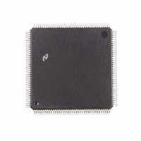
DP83907VF National Semiconductor, DP83907VF Datasheet - Page 13

DP83907VF
Manufacturer Part Number
DP83907VF
Description
IC CONTROLLR AT/LANII TP 160PQFP
Manufacturer
National Semiconductor
Datasheet
1.DP83907VF.pdf
(70 pages)
Specifications of DP83907VF
Controller Type
Network Interface Controller (NIC)
Interface
Twisted Pair
Voltage - Supply
4.75 V ~ 5.25 V
Current - Supply
150mA
Operating Temperature
0°C ~ 70°C
Mounting Type
Surface Mount
Package / Case
160-MQFP, 160-PQFP
Lead Free Status / RoHS Status
Contains lead / RoHS non-compliant
Other names
*DP83907VF
Available stocks
Company
Part Number
Manufacturer
Quantity
Price
Company:
Part Number:
DP83907VF
Manufacturer:
NSC
Quantity:
5 510
4 0 Functional Description
dure should be followed exactly and interrupts should be
disabled until it has completed to prevent any accidental
accesses to the DP83907
EEPROM LOAD()
4 4 JUMPERLESS OPERATION SUPPORT
One of the biggest problems in installing new adapters in a
PC is not knowing the available resources within that ma-
chine DP83907’s software configuration overcomes that
problem The conflicts possible in the I O base selection
can be overcome by a special mode for software configura-
tion of the I O base address By using this mode and by
using the configuration storage capability of the EEPROM a
fully software configurable design on the ISA bus can be
realized without address conflict problems
This mode is invoked by having the DP83907 default to
jumperless software configuration option in the I O base
selection This mode enables configuration register A to be
mapped to address location 278H which is defined to be a
printer port’s data register If software writes to this location
four consecutive times on the fourth write the DP83907 will
load the data written into the I O address bits of Configura-
tion Register A This data should set the I O base address
to a known conflict-free value The DP83907 can now be
configured and operated at the desired base I O address If
desired
EEPROM content to the new values eliminating the need to
reconfigure upon each power up Alternately the software
could leave the EEPROM alone and execute the configura-
tion using the printer port’s data register upon each power
up This configuration scheme will only work once after
each power-up Therefore the user can not enable the
DP83907 from reserved mode change it back into reserved
mode and enable it again A power-on reset must occur
between the first time it is enabled from the reserved mode
and the second
4 5 ETHERNET CABLE CONFIGURATION
DP83907 offers the choice of all the possible Ethernet ca-
bling options that is Ethernet (10BASE5) Thin Ethernet
(10BASE2) and Twisted-pair Ethernet (10BASE-T) The
the configuration software could change the
DISABLE INTERRUPTS()
value
value
value
WRITE(CONFIG B
READ(CONFIG B)
WRITE(CONFIG B
WRITE(CONFIG B
WRITE(CONFIG B
while (value AND EELOAD)
ENABLE INTERRUPTS()
READ(CONFIG B)
value AND
value OR EELOAD
value
WAIT()
value)
config for A)
config for B)
config for C)
READ(CONFIG B)
GDLINK
(Continued)
13
type of cabling used is controlled by Configuration Register
B DP83907 also supplies a THIN output signal which can
be used to disable enable an external DC-DC converter
which is required for 10BASE2
4 6 INTERRUPT AND LED OPERATION
The DP83907 has only one Interrupt Mode There are 8
possible interrupts Configuration Register A controls which
of the 8 interrupt lines are driven the others are TRI-STATE
The interrupt outputs should be connected to the fol-
lowing ISA Interrupt lines In the order given to main-
tain NE2000 Architecture compatibility 3 4 5 9 10 11
12 15
4 7 BOOT PROM OPERATION
The DP83907 supports an optional boot PROM the ad-
dress and size of which can be set in Configuration Register
C This boot PROM can be any 8-bit wide storage device
implemented with a non-volatile technology Write cycles to
this device can be enabled and disabled by programming
Configuration Register B This can be used to prevent un-
wanted write cycles to certain devices such as a Flash
EEPROM The DP83907 supplies the chip select to the de-
vice and buffers the data on to and from the ISA bus so the
memory support data bus should be connected to the boot
PROM’s data pins
4 8 DP8390 CORE (NETWORK INTERFACE CONTROL-
LER)
The DP8390 Core logic Figure 12 contains the Serializer
Deserializer which is controlled by the Protocol PLA DMA
Control FIFO Address Comparator and Multicast Hashing
Register The DP8390 core implements all of the IEEE
802 3 Media access control functions for the DP83907 and
interfaces to the internal ENDEC (on the left of the block
diagram) and to the Bus Interface and memory support bus
via a number of address data and control signals (the right
side of the block diagram) The following sections describe
the functions of the DP8390 core
Receive Deseriallzer
The Receive Deserializer is activated when the input signal
Carrier Sense is asserted to allow incoming bits to be shift-
ed into the shift register by the receive clock The serial
receive data is also routed to the CRC generator checker
The Receive Deserializer includes a synch detector which
detects the SFD (Start of Frame Delimiter) to establish
where byte boundaries within the serial bit stream are locat-
ed After every eight receive clocks the byte wide data is
transferred to the 16-byte FIFO and the Receive Byte Count
is incremented The first six bytes after the SFD are
checked for valid comparison by the Address Recognition
Logic If the Address Recognition Logic does not recognize
the packet the FlFO is cleared
CRC Generator Checker
During transmission the CRC logic generates a local CRC
field for the transmitted bit sequence The CRC encodes all
fields after the SFD The CRC is shifted out MSB first follow-


