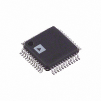
AD1981BJSTZ Analog Devices Inc, AD1981BJSTZ Datasheet - Page 27

AD1981BJSTZ
Manufacturer Part Number
AD1981BJSTZ
Description
IC CODEC STEREO MICPREAMP 48LQFP
Manufacturer
Analog Devices Inc
Series
SoundMAX®r
Type
Audio Codec '97r
Datasheet
1.AD1981BJST.pdf
(32 pages)
Specifications of AD1981BJSTZ
Data Interface
Serial
Resolution (bits)
16, 20 b
Number Of Adcs / Dacs
4 / 2
Sigma Delta
No
Dynamic Range, Adcs / Dacs (db) Typ
85 / 90
Voltage - Supply, Analog
4.5 V ~ 5.5 V
Voltage - Supply, Digital
3 V ~ 3.47 V
Operating Temperature
0°C ~ 70°C
Mounting Type
Surface Mount
Package / Case
48-LQFP
Single Supply Voltage (typ)
3.3/5V
Single Supply Voltage (min)
3/4.5V
Single Supply Voltage (max)
3.47/5.5V
Package Type
LQFP
Lead Free Status / RoHS Status
Lead free / RoHS Compliant
Available stocks
Company
Part Number
Manufacturer
Quantity
Price
Company:
Part Number:
AD1981BJSTZ
Manufacturer:
ADI
Quantity:
4
Company:
Part Number:
AD1981BJSTZ
Manufacturer:
AD
Quantity:
15
Part Number:
AD1981BJSTZ
Manufacturer:
ADI/亚德诺
Quantity:
20 000
Part Number:
AD1981BJSTZ-REEL
Manufacturer:
ADI/亚德诺
Quantity:
20 000
JACK SENSE/AUDIO INTERRUPT/STATUS REGISTER
Index 0x72
Reg
No.
0x72
Table 40.
Bit
JS0INT
JS1INT
JS0ST
JS1ST
JS0MD
JS1MD
JS0TMR
JS1TMR
JS0EQB
JS1EQB
JSMT [2:0]
All registers are not shown, and bits containing an X are assumed to be reserved.
All register bits are read/write except for JS0ST and JS1ST, which are read-only.
Name
Jack
Sense
Mnemonic
JS0 Interrupt
Js1 Interrupt
JS0 State
JS1 State
JS0 Mode
JS1 Mode
JS0 Timer Enable
JS1 Timer Enable
JS0 EQ Bypass Enable
JS1 EQ Bypass Enable
JS Mute Enable
Selector
D15
X
D14
X
D13
X
D12
JS
MT2
Function
This bit indicates that Pin JS0 has generated an interrupt. This bit remains set until the software
services the JS0 interrupt, that is, JS0 ISR should clear this bit by writing a 0 to it.
The interrupt to the system is an OR combination of this bit and JS1INT.
The actual interrupt implementation is selected by the INTS bit (Register 0x76). It is also possible to
generate a software system interrupt by writing a 1 to this bit.
This bit indicates that Pin JS1 has generated an interrupt. This bit remains set until the software
services the JS1 interrupt, that is, JS1 ISR should clear this bit by writing a 0 to it. See the JS0INT
description for details.
This bit always reports the logic state of the JS0 pin.
This bit always reports the logic state of the JS1 pin.
This bit selects the operation mode for the JS0 pin.
0 = Jack sense mode (default).
1 = Interrupt mode.
This bit selects the operation mode for the JS1 pin.
0 = Jack sense mode (default).
1 = Interrupt mode.
If this bit is set to 1, JS0 must be high for >278 ms to be recognized.
If this bit is set to 1, JS1 must be high for >278 ms to be recognized.
This bit enables JS0 to control the EQ bypass. When this bit is set to 1, JS0 = 1 causes the EQ to be
bypassed.
This bit enables JS1 to control the EQ bypass. When this bit is set to 1, JS1 = 1 causes the EQ to be
bypassed.
These three bits select and enable the jack sense muting action (see Table 41).
D11
JS
MT1
D10
JS
MT0
D9
JS1
EQB
Rev. C | Page 27 of 32
D8
JS0
EQB
D7
JS1
TMR
D6
JS0
TMR
D5
JS1
MD
D4
JS0
MD
D3
JS1
ST
D2
JS0
ST
D1
JS1
INT
AD1981B
D0
JS0
INT
Default
0x0000


