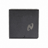
DP8344BV National Semiconductor, DP8344BV Datasheet - Page 41

DP8344BV
Manufacturer Part Number
DP8344BV
Description
IC BIPHASE COMM PROCESSR 84-PLCC
Manufacturer
National Semiconductor
Datasheet
1.DP8344BV.pdf
(184 pages)
Specifications of DP8344BV
Processor Type
8-Bit RISC
Speed
20MHz
Voltage
4.5 ~ 5.5V
Mounting Type
Surface Mount
Package / Case
84-PLCC
Operating Supply Voltage (typ)
5V
Operating Supply Voltage (max)
5.5V
Operating Supply Voltage (min)
4.5V
Mounting
Surface Mount
Operating Temperature (max)
70C
Operating Temperature (min)
0C
Operating Temperature Classification
Commercial
Lead Free Status / RoHS Status
Contains lead / RoHS non-compliant
Features
-
Lead Free Status / Rohs Status
Not Compliant
Other names
*DP8344BV
Available stocks
Company
Part Number
Manufacturer
Quantity
Price
Company:
Part Number:
DP8344BV
Manufacturer:
NSC
Quantity:
5 510
Part Number:
DP8344BV
Manufacturer:
NS/国半
Quantity:
20 000
Figure 2-32 ICLK rises on the rising edge of CPU-CLK one
2 0 CPU Description
The CPU will be stopped after RESET is asserted low The
CPU can be externally controlled by changing the state of
the start bit
instructions from the current address in the program control
register when a one is written to STRT and stops when
struction before stopping Controlling the CPU from RIC
requires a processor to access RIC If no external proces-
sor is present the CPU can be made to start automatically
after reset by holding REM-WR and REM-RD low and RAE
high while RESET is transitioning from low to high The CPU
‘‘kick-starts’’ and will begin executing instructions from ad-
dress zero The timing for kick-starting the CPU is shown in
T-state after RESET is de-asserted The falling edge of
ICLK signifies the beginning of the first instruction fetch
Three instruction wait states and T2 precede the first in-
struction
A functional state diagram describing the timing of the CPU
is shown in Figure 2-33 The functional state diagram is sim-
ilar to a flow chart except that transitions to a new state
(states are denoted as rectangular boxes) can only occur on
the rising edge of the CPU-CLK A state box can specify
several actions and each action is separated by a horizon-
tal line A signal name listed in a state box indicates that that
pin will be asserted high when Timing Control has entered
that state When the signal is omitted from a box it is as-
serted low (Note this requires using the inversion of a sig-
nal in some cases ) Decision blocks are shown as diamonds
and their meaning is the same as in a flow chart The func-
tional state diagram is a generalized approach to determin-
ing instruction flow while allowing for any combination of
wait states and control signals Timing Control always starts
from a reset in the state IDLE After RESET goes high Tim-
ing Control remains in IDLE until STRT is written high If
the BCP kick-starts Timing Control enters TST on the next
rising edge of CPU-CLK Timing Control starts with a dummy
STRT is cleared The CPU will complete the current in-
STRT
in RIC
The CPU starts executing
(Continued)
FIGURE 2-32 CPU Start-Up Timing
41
ure 2-21 Any instruction cycle can be analyzed in a similar
instruction cycle in order to fetch the first instruction ICLK
goes high in T1 and the instruction wait state counter is
loaded ICLK falls when either T2 or TW is entered as deter-
mined by the value of i
flow begins after T2 at B on the diagram As an example
consider a three T-state data memory write instruction with
one data wait state The instruction cycle path for this in-
struction would begin at T1 following the decision block for
data memory access In T1 ICLK is asserted high the in-
struction wait state counter is loaded and a bus request to
RIAS is generated Also ALE is asserted high on the falling
edge of CPU-CLK during T1 A branch decision is now made
based on the state of LOCK and the response from RIAS to
the bus request Assuming that LOCK is not asserted and a
remote access is not in progress Timing Control enters TX
on the next rising edge of CPU-CLK In TX the data wait
state counter is loaded and the instruction wait state coun-
ter is decremented In this example the instruction wait
state counter is at zero and is not counting The data wait
state counter is loaded with one ALE goes low on the fall-
ing edge of CPU-CLK during TX The next decision block
checks for a read of data memory This example is a write to
data memory so the decision is no and the branch is to the
right The wait state conditions are evaluated in the follow-
ing decision block i
on the next rising edge of CPU-CLK WRITE is asserted low
when TW is entered and the data wait state counter is dec-
remented to zero The decision on i
now true and T2 is entered on the next rising edge of CPU-
CLK WRITE remains low The CPU will stop execution if
struction will be executed beginning at A To summarize
this instruction went through the following states T1 TX
TW and T2 The complete instruction cycle is shown in Fig-
manner using this functional state diagram
STRT is low at B in the diagram Otherwise the next in-
DW
IW
is one and Timing Control enters TW
and WAIT The normal instruction
DW
i
IW
and WAIT is
TL F 9336 – F5


