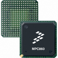
MPC885CVR133 Freescale Semiconductor, MPC885CVR133 Datasheet - Page 9

MPC885CVR133
Manufacturer Part Number
MPC885CVR133
Description
IC MPU POWERQUICC 133MHZ 357PBGA
Manufacturer
Freescale Semiconductor
Datasheet
1.MPC880VR80.pdf
(87 pages)
Specifications of MPC885CVR133
Processor Type
MPC8xx PowerQUICC 32-Bit
Speed
133MHz
Voltage
3.3V
Mounting Type
Surface Mount
Package / Case
357-PBGA
Processor Series
MPC8xx
Core
MPC8xx
Data Bus Width
32 bit
Maximum Clock Frequency
133 MHz
Operating Supply Voltage
0 V to 5 V
Maximum Operating Temperature
+ 95 C
Mounting Style
SMD/SMT
Data Ram Size
8 KB
I/o Voltage
5 V
Interface Type
I2C, SPI, UART
Minimum Operating Temperature
0 C
Program Memory Size
8 KB
Program Memory Type
EPROM/Flash
For Use With
CWH-PPC-885XN-VX - BOARD EVAL QUICCSTART MPC885CWH-PPC-885XN-VE - BOARD EVAL QUICCSTART MPC885
Lead Free Status / RoHS Status
Lead free / RoHS Compliant
Features
-
Lead Free Status / Rohs Status
Lead free / RoHS Compliant
Available stocks
Company
Part Number
Manufacturer
Quantity
Price
Company:
Part Number:
MPC885CVR133
Manufacturer:
Freescale Semiconductor
Quantity:
135
Company:
Part Number:
MPC885CVR133
Manufacturer:
MOTOROLA
Quantity:
745
Company:
Part Number:
MPC885CVR133
Manufacturer:
Freescale Semiconductor
Quantity:
10 000
3
This section provides the maximum tolerated voltage and temperature ranges for the MPC885/MPC880.
Table 2
1
2
Figure 3
Freescale Semiconductor
Supply voltage
Input voltage
Storage temperature range
The power supply of the device must start its ramp from 0.0 V.
Functional operating conditions are provided with the DC electrical specifications in
stress ratings only; functional operation at the maxima is not guaranteed. Stress beyond those listed may affect device
reliability or cause permanent damage to the device. See
Caution: All inputs that tolerate 5 V cannot be more than 2.5 V greater than V
normal operation (that is, if the MPC885/MPC880 is unpowered, a voltage greater than 2.5 V must not be applied to its inputs).
Maximum Tolerated Ratings
displays the maximum tolerated ratings, and
shows the undershoot and overshoot voltages at the interfaces of the MPC885/MPC880.
2
1
Rating
V
Note:
V
1. t
IH
IL
interface
V
Figure 3. Undershoot/Overshoot Voltage for V
V
DDH
MPC885/MPC880 PowerQUICC Hardware Specifications, Rev. 7
DDH
/V
GND – 0.3 V
GND – 0.7 V
refers to the clock period associated with the bus clock interface.
/V
V
DDL
DDH
DDL
+ 20%
/V
+ 5%
GND
Table 2. Maximum Tolerated Ratings
DDL
Difference between V
Section 8, “Power Supply and Power Sequencing.”
Table 3
VDDSYN
Symbol
Not to Exceed 10%
V
V
T
V
DDH
DDL
stg
in
of t
DDL
interface
displays the operating temperatures.
and V
1
DDH
DDSYN
DDH
. This restriction applies to power up and
Table
and V
6. Absolute maximum ratings are
DDL
GND – 0.3 to V
–55 to +150
–0.3 to 4.0
–0.3 to 2.0
–0.3 to 2.0
Maximum Tolerated Ratings
Value
<100
DDH
Unit
mV
°C
V
V
V
V
9


