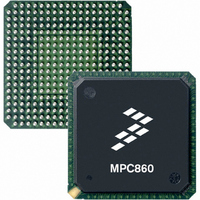
MPC885CVR133 Freescale Semiconductor, MPC885CVR133 Datasheet - Page 37

MPC885CVR133
Manufacturer Part Number
MPC885CVR133
Description
IC MPU POWERQUICC 133MHZ 357PBGA
Manufacturer
Freescale Semiconductor
Datasheet
1.MPC880VR80.pdf
(87 pages)
Specifications of MPC885CVR133
Processor Type
MPC8xx PowerQUICC 32-Bit
Speed
133MHz
Voltage
3.3V
Mounting Type
Surface Mount
Package / Case
357-PBGA
Processor Series
MPC8xx
Core
MPC8xx
Data Bus Width
32 bit
Maximum Clock Frequency
133 MHz
Operating Supply Voltage
0 V to 5 V
Maximum Operating Temperature
+ 95 C
Mounting Style
SMD/SMT
Data Ram Size
8 KB
I/o Voltage
5 V
Interface Type
I2C, SPI, UART
Minimum Operating Temperature
0 C
Program Memory Size
8 KB
Program Memory Type
EPROM/Flash
For Use With
CWH-PPC-885XN-VX - BOARD EVAL QUICCSTART MPC885CWH-PPC-885XN-VE - BOARD EVAL QUICCSTART MPC885
Lead Free Status / RoHS Status
Lead free / RoHS Compliant
Features
-
Lead Free Status / Rohs Status
Lead free / RoHS Compliant
Available stocks
Company
Part Number
Manufacturer
Quantity
Price
Company:
Part Number:
MPC885CVR133
Manufacturer:
Freescale Semiconductor
Quantity:
135
Company:
Part Number:
MPC885CVR133
Manufacturer:
MOTOROLA
Quantity:
745
Company:
Part Number:
MPC885CVR133
Manufacturer:
Freescale Semiconductor
Quantity:
10 000
Table 11
1
Freescale Semiconductor
Num
P44 A(0:31), REG valid to PCMCIA strobe
P45 A(0:31), REG valid to ALE negation
P46 CLKOUT to REG valid
P47 CLKOUT to REG invalid
P48 CLKOUT to CE1, CE2 asserted
P49 CLKOUT to CE1, CE2 negated
P50 CLKOUT to PCOE, IORD, PCWE, IOWR
P51 CLKOUT to PCOE, IORD, PCWE, IOWR
P52 CLKOUT to ALE assert time
P53 CLKOUT to ALE negate time
P54 PCWE, IOWR negated to D(0:31) invalid
P55 WAITA and WAITB valid to CLKOUT rising
P56 CLKOUT rising edge to WAITA and WAITB
PSST = 1. Otherwise add PSST times cycle time.
PSHT = 0. Otherwise add PSHT times cycle time.
These synchronous timings define when the WAITx signals are detected in order to freeze (or relieve) the PCMCIA current
cycle. The WAITx assertion will be effective only if it is detected 2 cycles before the PSL timer expiration. See Chapter 16,
“PCMCIA Interface,” in the MPC885 PowerQUICC™ Family Reference Manual .
asserted
(MIN = 1.00 × B1 – 2.00)
(MAX = 0.25 × B1 + 8.00)
(MIN = 0.25 – B1 + 1.00)
(MAX = 0.25 × B1 + 8.00)
(MAX = 0.25 × B1 + 8.00)
assert time (MAX = 0.00 × B1 + 11.00)
negate time (MAX = 0.00 × B1 + 11.00)
(MAX = 0.25 × B1 + 6.30)
(MAX = 0.25 × B1 + 8.00)
(MIN = 0.25 × B1 – 2.00)
edge
invalid
shows the PCMCIA timing for the MPC885/MPC880.
1
1
(MIN = 0.00 × B1 + 8.00)
(MIN = 0.00 × B1 + 2.00)
1
(MIN = 0.75 × B1 – 2.00)
Characteristic
MPC885/MPC880 PowerQUICC Hardware Specifications, Rev. 7
1
Table 11. PCMCIA Timing
1
20.70
28.30
7.60
8.60
7.60
7.60
2.00
7.60
5.60
8.00
2.00
Min
—
—
33 MHz
15.60
15.60
15.60
11.00
11.00
13.80
15.60
Max
—
—
—
—
—
—
16.70
23.00
6.30
7.30
6.30
6.30
2.00
6.30
4.30
8.00
2.00
Min
—
—
40 MHz
14.30
14.30
14.30
11.00
11.00
12.50
14.30
Max
—
—
—
—
—
—
13.20
9.40
3.80
4.80
3.80
3.80
2.00
3.80
1.80
8.00
2.00
Min
—
—
66 MHz
11.80
11.80
11.80
11.00
11.00
10.00
11.80
Max
—
—
—
—
—
—
10.50
7.40
3.13
4.13
3.13
3.13
2.00
3.13
1.13
8.00
2.00
Min
—
—
80 MHz
Bus Signal Timing
11.13
11.13
11.13
11.00
11.00
11.13
Max
9.40
—
—
—
—
—
—
Unit
ns
ns
ns
ns
ns
ns
ns
ns
ns
ns
ns
ns
ns
37


